| Place of Origin: | China |
|---|---|
| Brand Name: | CESGATE |
| Certification: | UL、IATF16949、ISO9001 |
| Model Number: | N/A |
| Minimum Order Quantity: | 1PCS( NO MOQ) |
| Price: | Negotiable (Depends on your GERBER and BOM) |
| Packaging Details: | PCB: Vacuum Packing / PCBA: ESD Packing |
| Delivery Time: | 1-30 working days |
| Payment Terms: | T/T, L/C |
| Supply Ability: | 30,000pcs/month |
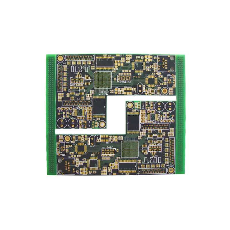
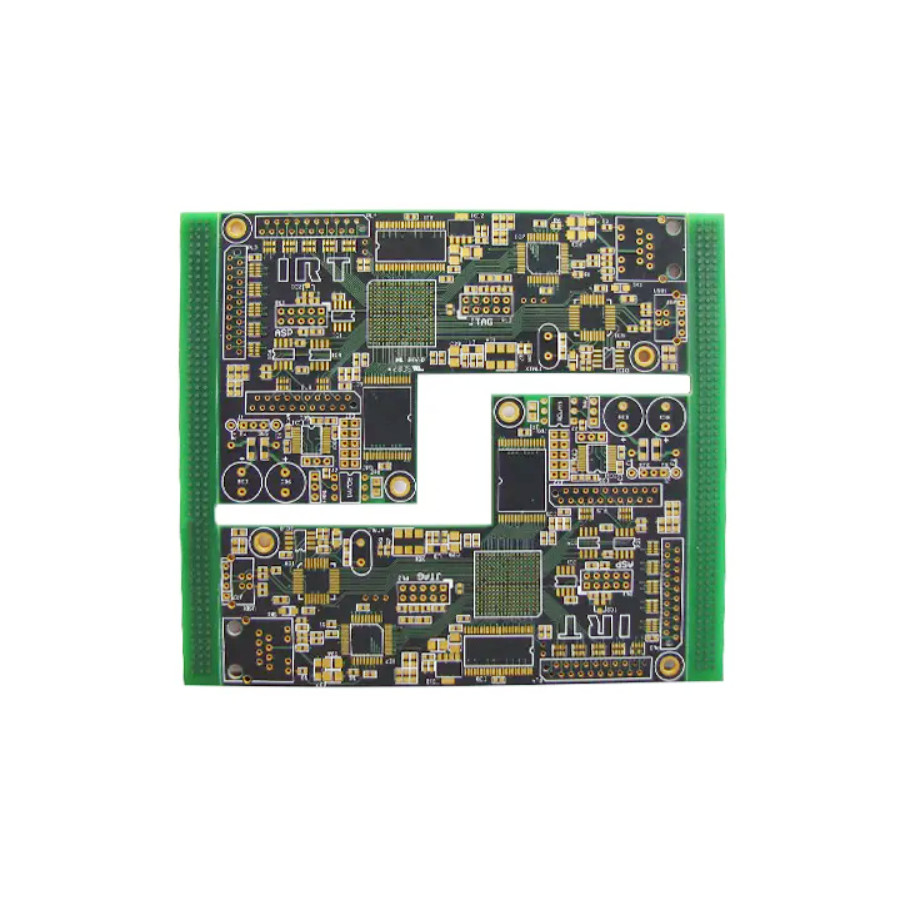
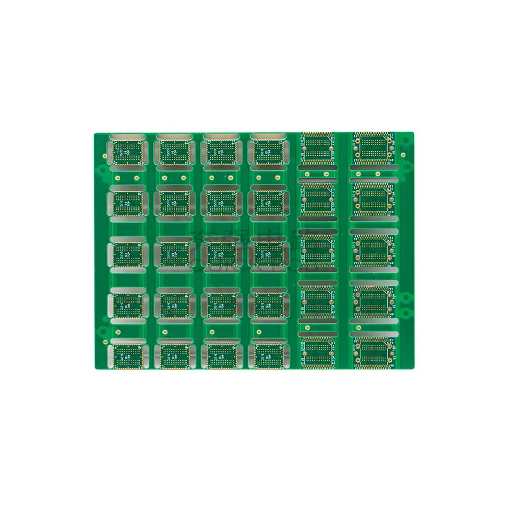
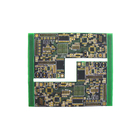
| Product Name: | Soldering Small Circuit Boards Smd Pcb FUJI NXT3 HDI PCB Soldering Pads | Feature: | Soldering Small Circuit Boards |
|---|---|---|---|
| Base Material: | FR-4, TACONIC, Aluminum, CEM-3, Metal/ceramic/aluminum Base | Min. Line Spacing: | 1.6mm, 0.2-6.0mm, 0.2mm-6.00 Mm(8mil-126mil), 0.5~3.2mm, 1.6 Mm |
| Application: | Electronics Device, Consumer Electronics, Communications, And So On, Universal | Solder Mask Color: | Green, Blue, White And Red, White Black Yellow Green Red, Purple |
| Testing Service: | 100% Electrical Test, Fly-probe, Function Testing, 100% E-testing, Flying Probe Testing | Copper Thickness: | 1oz, 0.5oz-8oz, 1/3oz ~6oz, 1 Oz, 0.25OZ~12OZ |
| Material: | FR4/94v0/Aluminum/cem-1 Cem-3/, FR4, FR4 CEM1 CEM3 Hight TG | ||
| High Light: | Soldering Circuit Boards Smd Pcb,FUJI NXT3 HDI PCB |
||
Soldering Small Circuit Boards Smd Pcb FUJI NXT3 HDI PCB Soldering Pads
CESGATE provides Electronic Manufacturing Services (EMS) for your products that require surface mount, through hole, BGA and mixed technology.
Our main services include HDI PCB assembly (Electronic assembly), component procurement and PCB fabrication from quick turn, sample run to volume production.
Our customers are who of the Medical, Instrumentation, Intelligent home, Automotive, Consumer electronics industry and Robotics industries.
Full range of HDI PCB manufacturing and assembly services to fit all of your printed circuit board needs.
Rigid-flex board refers to pressing the flexible circuit board and the rigid circuit board together according to the relevant process requirements during PCB proofing to form a circuit board with FPC characteristics and PCB characteristics; its price is relatively high, but its use Extremely broad and can be tailored for applications in many industries. So, under what circumstances does PCB proofing need to use rigid-flex board?
1. High impact and high vibration environment. The rigid-flex board has strong impact resistance and can be used in high stress environments to ensure stable performance of the equipment, otherwise it will cause equipment failure.
2. High-precision applications where reliability is more important than cost considerations. If a cable or connector failure is dangerous, it is better to use a more durable flex-rigid board.
3. High density applications. Some components lack the surface area required for all necessary connectors and cables. In this case, using a flexible rigid board can save space to solve this problem.
4. Applications requiring multiple rigid boards. When more than four connection boards are included in the assembly, replacing them with a single rigid-flex board may be the best option and more cost-effective.
Types and uses of HDI PCB
(A) 4-layer board
The substrate material is mainly epoxy glass fiber cloth. The main uses are personal computers, medical electronic equipment, measuring instruments, semiconductor testing machines, numerical control machines, electronic switches, communication machines, memory circuit boards, IC cards, etc.
(B) 6-8 layer board
The substrate material is still mainly epoxy resin glass fiber cloth. Most of them are used in electronic switches, semiconductor testing machines, mid-range personal computers, engineering workstations and other machines.
(C) 10 layers or more
The material is mainly glass benzene resin material, or epoxy resin is used as the multi-layer PCB substrate material. The application of this type of PCB is special, and it is used in large industrial computers, high-speed computers, defense machines, communication machines, etc.
PCB Capacities and Technical Specification
| NO. | Items | Capabilities |
| 1 | Layers | 2-68L |
| 2 | Maximum machining size | 600mm*1200mm |
| 3 | Board thickness | 0.2mm-6.5mm |
| 4 | Copper thickness | 0.5oz-28oz |
| 5 | Min trace/space | 2.0mil/2.0mil |
| 6 | Minimum finished aperture | 0. 10mm |
| 7 | Maximum thickness to diameter ratio | 15:1 |
| 8 | Via treatment | Via, blind&buried via, via in pad, Copper in via … |
| 9 | Surface finish/treatment | HASL/HASL lead free, Chemical tin, Chemical Gold, Immersion gold Inmersion Silver/Gold, Osp, Gold Plating |
| 10 | Base Material | FR408 FR408HR, PCL-370HR;IT180A, Megtron 6(Panasonic);Rogers4350, Rogers4003, RO3003, Rogers/Taconic/Arlon/Nelco laminate with FR-4 material(including partial Ro4350B hybrid laminating with FR-4) |
| 11 | Solder mask color | Green.Black.Red.Yellow.White.Blue.Purple.Matte Green. Matte Black |
| 12 | Testing Service | AOI, X-Ray, Flying-Probe, Function Test, First Article Tester |
| 13 | Profiling Punching | Routing,V-CUT,Beveling |
| 14 | Bow&twist | ≤0.5% |
| 15 | HDI type | 1+n+1,2+n+2,3+n+3 |
| 16 | Min mechanical aperture | 0.1mm |
| 17 | Min laser aperture | 0.075mm |
Welcome to Chengdu Cesgate Technology Co., Ltd
We can provide one-stop service:
PCB circuit boards+Assembly
E-test.
Electronic components purchasing.
PCB assembly: available on SMT, BGA, DIP.
PCBA function test.
Enclosure assembly.
![]()
![]()
![]()
![]()
![]()
![]()
![]()
FAQ
| Q: Why choose us? CESGATE: Professional and experienced R&D team. Advanced production equipment, scientific and reasonable process flow. Reliable and strict quality control system. We test all our products before shipment to make sure everything is in perfect condition. |
| Q: How long does it take for PCB quote? CESGATE: Normally 12 hours to 48 hours as soon as receive internal engineer evaluate confirmation. |
| Q: The Wire Bonding process is required when the circuit board is printed. What should I pay attention to when making the circuit board? CESGATE: When making circuit boards, the surface treatment options are mostly "nickel palladium gold ENEPIG" or "chemical gold ENIG". If the Al aluminum wire is used, the gold thickness is recommended to be 3μ”~5μ”, but if the Au gold wire is used, the gold thickness should preferably be more than 5μ”. |
| Q: The lead-free process is required when the circuit board is printed. What should I pay attention to when making the circuit board? CESGATE: The lead-free process during printing is higher than the temperature resistance requirements of the general process, and the temperature resistance requirements must be above 260 °C. Therefore, it is recommended to use a substrate above TG150 when selecting the substrate material. |