| Place of Origin: | China |
|---|---|
| Brand Name: | CESGATE |
| Certification: | UL、IATF16949、ISO9001 |
| Model Number: | N/A |
| Minimum Order Quantity: | 1PCS( NO MOQ) |
| Price: | Negotiable (Depends on your GERBER and BOM) |
| Packaging Details: | PCB: Vacuum Packing / PCBA: ESD Packing |
| Delivery Time: | 1-30 working days |
| Payment Terms: | T/T, L/C |
| Supply Ability: | 30,000pcs/month |
| Product Name: | Emergency Light Circuit Board Turn Key Assembly HDI PCB Netsuite Advanced Bom | Feature: | Netsuite Advanced Bom |
|---|---|---|---|
| Surface Finishing: | HASL-LF/OSP/ENIG Etc | Solder Mask: | Green, White Black Green Blue Red, Green Or Other Color As You Want, Green/blue, Green Black Bule White |
| Certificate: | ISO9001/Iso14001/CE/ROHS | Testing Service: | 100% Electrical Test, Fly-probe, Function Testing, 100% E-testing, Flying Probe Testing |
| Shipping: | DHL UPS TNT Fedex EMS | Type Of Services: | Custom Electronic Pcb Service |
| High Light: | Fly probe Emergency Light Circuit Board,Emergency Light Circuit Board Nelco laminate,Fly probe HDI PCB |
||
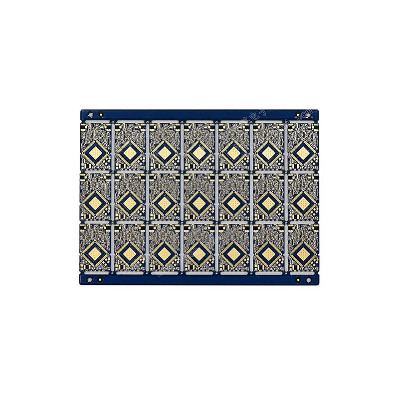
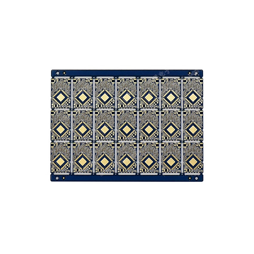
Emergency Light Circuit Board Turn Key Assembly HDI PCB Netsuite Advanced Bom
PCB Inspection Method
PCB inspection methods include appearance optical inspection and electrical path test
AOI (Auto Optical Inspection):
It is the automatic optical recognition system. Based on the consideration of production efficiency and inspection accuracy, the use of optical identification instruments to replace manual visual inspection (Visual Inspection) is already a very basic process. The principle of AOI is to first save the standard image file in the device, use the image file to perform optical comparison with the measured object, and automatically determine whether the error of the measured object exceeds the standard. Scrap or repair. Since the circuits on the circuit boards are getting more and more fine, it has already exceeded the limit that can be found by the human eye. Therefore, the AOI equipment of the HDI PCB is mostly used to check and compare the circuit layers, and compare whether there is too much or too little etching or damage such as collisions. .
Industrial Application
High-power industrial applications of HDI PCBs are common. These electronic components control the mechanisms used in factories and manufacturing facilities and must withstand the harsh conditions commonly found in industrial installations. This can include anything including harsh chemicals, vibrating machinery and rough handling.
In such a rapidly challenging environment, industry standards are equally stringent. Currently, thick copper HDI PCBs (much thicker than standard ounce PCBs) are often seen in other applications. This HDI PCB is helpful for high current industrial applications and battery chargers.
1. Industrial Equipment: Many drills and presses used in manufacturing operate using HDI PCB-controlled electronics.
2. Measuring Equipment: Equipment used to measure and control pressure, temperature and other variables in industrial manufacturing processes.
3. Power equipment: DC-AC power inverter, solar cogeneration equipment and other power control equipment.
PCB Capacities and Technical Specification
| NO. | Items | Capabilities |
| 1 | Layers | 2-68L |
| 2 | Maximum machining size | 600mm*1200mm |
| 3 | Board thickness | 0.2mm-6.5mm |
| 4 | Copper thickness | 0.5oz-28oz |
| 5 | Min trace/space | 2.0mil/2.0mil |
| 6 | Minimum finished aperture | 0. 10mm |
| 7 | Maximum thickness to diameter ratio | 15:1 |
| 8 | Via treatment | Via, blind&buried via, via in pad, Copper in via … |
| 9 | Surface finish/treatment | HASL/HASL lead free, Chemical tin, Chemical Gold, Immersion gold Inmersion Silver/Gold, Osp, Gold Plating |
| 10 | Base Material | FR408 FR408HR, PCL-370HR;IT180A, Megtron 6(Panasonic);Rogers4350, Rogers4003, RO3003, Rogers/Taconic/Arlon/Nelco laminate with FR-4 material(including partial Ro4350B hybrid laminating with FR-4) |
| 11 | Solder mask color | Green.Black.Red.Yellow.White.Blue.Purple.Matte Green. Matte Black |
| 12 | Testing Service | AOI, X-Ray, Flying-Probe, Function Test, First Article Tester |
| 13 | Profiling Punching | Routing,V-CUT,Beveling |
| 14 | Bow&twist | ≤0.5% |
| 15 | HDI type | 1+n+1,2+n+2,3+n+3 |
| 16 | Min mechanical aperture | 0.1mm |
| 17 | Min laser aperture | 0.075mm |
Welcome to Chengdu Cesgate Technology Co., Ltd
We can provide one-stop service:
PCB circuit boards+Assembly
E-test.
Electronic components purchasing.
PCB assembly: available on SMT, BGA, DIP.
PCBA function test.
Enclosure assembly.
![]()
![]()
![]()
![]()
![]()
![]()
![]()
FAQ
| Q: What is your inspection policy? How do you control the quality? CESGATE: In order to ensure the quality of PCB products, flying probe inspection is usually used; electrical fixtures, automatic optical inspection (AOI), BGA parts x-ray inspection, first article inspection ( FAI) etc. |
| Q: The lead-free process is required when the circuit board is printed. What should I pay attention to when making the circuit board? CESGATE: The lead-free process during printing is higher than the temperature resistance requirements of the general process, and the temperature resistance requirements must be above 260 °C. Therefore, it is recommended to use a substrate above TG150 when selecting the substrate material. |
| Q: Popular field? CESGATE: Semiconductor, Smart Home, Medical Products, Smart Wearable, Industrial Control, IOT etc. |
| Q: Which express companies do you cooperate with? CESGATE: We cooperate with express companies, including DHL, FedEX, UPS, TNT and EMS. And we also have our own freight forwarders, with lower shipping fees. |
| Q: What is the difference between the HDI board and the general circuit board? CESGATE: Most of HDI use laser to form holes, while general circuit boards only use mechanical drilling, and HDI boards are manufactured by the build-up method (Build Up), so more layers will be added, while general circuit boards are only added once. |