

| Place of Origin: | China |
|---|---|
| Brand Name: | CESGATE |
| Certification: | UL、IATF16949、ISO9001 |
| Model Number: | N/A |
| Minimum Order Quantity: | 1PCS( NO MOQ) |
| Price: | Negotiable (Depends on your GERBER and BOM) |
| Packaging Details: | PCB: Vacuum Packing / PCBA: ESD Packing |
| Delivery Time: | 1-30 working days |
| Payment Terms: | T/T, L/C |
| Supply Ability: | 30,000pcs/month |
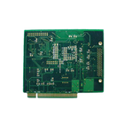
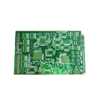
| Product Name: | Differential Pair Altium Medical Electronics Assembly HDI PCB Sap Pm Bom | Feature: | Differential Pair Altium |
|---|---|---|---|
| Surface Finishing: | HASL,Lead-free HASL ,OSP,Flash Gold,ENIG, | Solder Mask: | Green, White Black Green Blue Red, Green Or Other Color As You Want, Green/blue, Green Black Bule White |
| Certificate: | IATF16949/ISO13485/ISO9001/ISO14001 | Testing Service: | 100% Electrical Test, Fly-probe, Function Testing, 100% E-testing, Flying Probe Testing |
| PCB Outline: | Square,circle,irregular(with Jigs) | ||
| High Light: | Flash Gold ENIG medical device pcb,medical device pcb Lead free HASL,Flash Gold ENIG HDI PCB board |
||
Differential Pair Altium Medical Electronics Assembly HDI PCB Sap Pm Bom
PCB inspection method
PCB inspection methods include appearance optical inspection and electrical path test
AOI (Auto Optical Inspection):
It is the automatic optical recognition system. Based on the consideration of production efficiency and inspection accuracy, the use of optical identification instruments to replace manual visual inspection (Visual Inspection) is already a very basic process. The principle of AOI is to first save the standard image file in the device, use the image file to perform optical comparison with the measured object, and automatically determine whether the error of the measured object exceeds the standard. Scrap or repair. Since the circuits on the circuit boards are getting more and more fine, it has already exceeded the limit that can be found by the human eye. Therefore, the AOI equipment of the HDI PCB is mostly used to check and compare the circuit layers, and compare whether there is too much or too little etching or damage such as collisions. .
Application
Printed circuit boards (PCBs) are indispensable accessories in modern electronic devices. Printed circuit boards are used in all electronic equipment, whether it is large machinery or personal computers, communication base stations or mobile phones, household appliances or electronic toys. HDI PCBs are mainly composed of insulating substrates and conductors, which play the role of support, interconnection and part of circuit elements in electronic equipment. Electronic components such as integrated circuits, resistors, capacitors, etc. cannot function as a single entity. They only work as a whole if they have a firm foothold on the HDI PCB and there are conductive junctions connecting them. The printed circuit board is the skeleton that supports the components and is the conduit for connecting electrical signals. In addition, some printed circuit boards have components such as resistors, capacitors, inductors, etc., which become functional circuits and play the role of trachea.The role of printed circuit boards in electronic equipment is to provide mechanical support for fixing and assembling for transistors, integrated circuits, resistors, capacitors, inductors and other components; to realize the integration of transistors, integrated circuits, resistors, capacitors, inductors and other components. Wiring and electrical connection and electrical insulation between components meet their electrical characteristics; provide identification characters and graphics for the inspection and maintenance of components in the electronic assembly process, and provide solder resist graphics for wave soldering.
PCB Capacities and Technical Specification
| NO. | Items | Capabilities |
| 1 | Layers | 2-68L |
| 2 | Maximum machining size | 600mm*1200mm |
| 3 | Board thickness | 0.2mm-6.5mm |
| 4 | Copper thickness | 0.5oz-28oz |
| 5 | Min trace/space | 2.0mil/2.0mil |
| 6 | Minimum finished aperture | 0. 10mm |
| 7 | Maximum thickness to diameter ratio | 15:1 |
| 8 | Via treatment | Via, blind&buried via, via in pad, Copper in via … |
| 9 | Surface finish/treatment | HASL/HASL lead free, Chemical tin, Chemical Gold, Immersion gold Inmersion Silver/Gold, Osp, Gold Plating |
| 10 | Base Material | FR408 FR408HR, PCL-370HR;IT180A, Megtron 6(Panasonic);Rogers4350, Rogers4003, RO3003, Rogers/Taconic/Arlon/Nelco laminate with FR-4 material(including partial Ro4350B hybrid laminating with FR-4) |
| 11 | Solder mask color | Green.Black.Red.Yellow.White.Blue.Purple.Matte Green. Matte Black |
| 12 | Testing Service | AOI, X-Ray, Flying-Probe, Function Test, First Article Tester |
| 13 | Profiling Punching | Routing,V-CUT,Beveling |
| 14 | Bow&twist | ≤0.5% |
| 15 | HDI type | 1+n+1,2+n+2,3+n+3 |
| 16 | Min mechanical aperture | 0.1mm |
| 17 | Min laser aperture | 0.075mm |
Company introduction
CESGATE provides Electronic Manufacturing Services (EMS) for your products that require surface mount, through hole, BGA and mixed technology.Our main services include PCB assembly (Electronic assembly), component procurement and PCB fabrication from quick turn, sample run to volume production.Our customers are who of the Medical, Instrumentation, Intelligent home, Automotive, Consumer electronics industry and Robotics industries.Full range of PCB manufacturing and assembly services to fit all of your printed circuit board needs.CESGATE is the professional PCB and PCBA Manufacturer, can provide one-stop service from PCB/PCBA Design, PCB/PCBA Clone, PCB manufacturing, Components sourcing, PCB Assembly, and fully product assembly and test. We have got certification of ISO 9001, ISO 13485 and UL. Our capacity including: 1-32 layers FR4 PCB board manufacturing, 1-12 layers Flexible PCB manufacturing, Aluminum PCB and Ceramic PCB manufacturing, can finish about 324000pcs PCBA per months.
![]()
![]()
![]()
![]()
![]()
![]()
![]()
FAQ
| Q: What is needed for PCB & PCBA quotation? CESGATE: For PCB: Gerber file and technic requirements(material,size, surface finish treatment, copper thickness,board thickness) and quantity you need. For PCBA: Files mentioned above, BOM, pick and place file. |
| Q: What is your inspection policy? How do you control the quality? CESGATE: In order to ensure the quality of PCB products, flying probe inspection is usually used; electrical fixtures, automatic optical inspection (AOI), BGA parts x-ray inspection, first article inspection ( FAI) etc. |
| Q: The Wire Bonding process is required when the circuit board is printed. What should I pay attention to when making the circuit board? CESGATE: When making circuit boards, the surface treatment options are mostly "nickel palladium gold ENEPIG" or "chemical gold ENIG". If the Al aluminum wire is used, the gold thickness is recommended to be 3μ”~5μ”, but if the Au gold wire is used, the gold thickness should preferably be more than 5μ”. |
| Q: How can we ensure our information should not let third party to see our design? CESGATE: We are willing to sign NDA effect by customer side local law and promising to keep customers data in high confidential level. |
| Q: Which express companies do you cooperate with? CESGATE: We cooperate with express companies, including DHL, FedEX, UPS, TNT and EMS. And we also have our own freight forwarders, with lower shipping fees. |


