| Place of Origin: | China |
|---|---|
| Brand Name: | CESGATE |
| Certification: | UL、IATF16949、ISO9001 |
| Model Number: | N/A |
| Minimum Order Quantity: | 1PCS( NO MOQ) |
| Price: | Negotiable (Depends on your GERBER and BOM) |
| Packaging Details: | PCB: Vacuum Packing / PCBA: ESD Packing |
| Delivery Time: | 1-30 working days |
| Payment Terms: | T/T, L/C |
| Supply Ability: | 30,000pcs/month |
| Product Name: | Differential Pair Altium Circuit Card Assy HDI PCB Solidworks Bom Template | Feature: | Differential Pair Altium Circuit |
|---|---|---|---|
| Base Material: | FR-4, TACONIC, Aluminum, CEM-3, Metal/ceramic/aluminum Base | Surface Finishing: | HASL, Chemical Tin, Chemical Gold, Immersion Gold, HASL |
| Solder Mask: | Green, White Black Green Blue Red, Green Or Other Color As You Want, Green/blue, Green Black Bule White | Application: | Electronics Device, Consumer Electronics, Communications, And So On, Universal |
| Copper Thickness Color: | 1/2 Oz Min; 12 Oz Max | Testing Service: | 100% Electrical Test, Fly-probe, Function Testing, 100% E-testing, Flying Probe Testing |
| High Light: | 0.5oz copper HDI circuit boards,Altium HDI circuit boards,0.5oz copper circuit board |
||
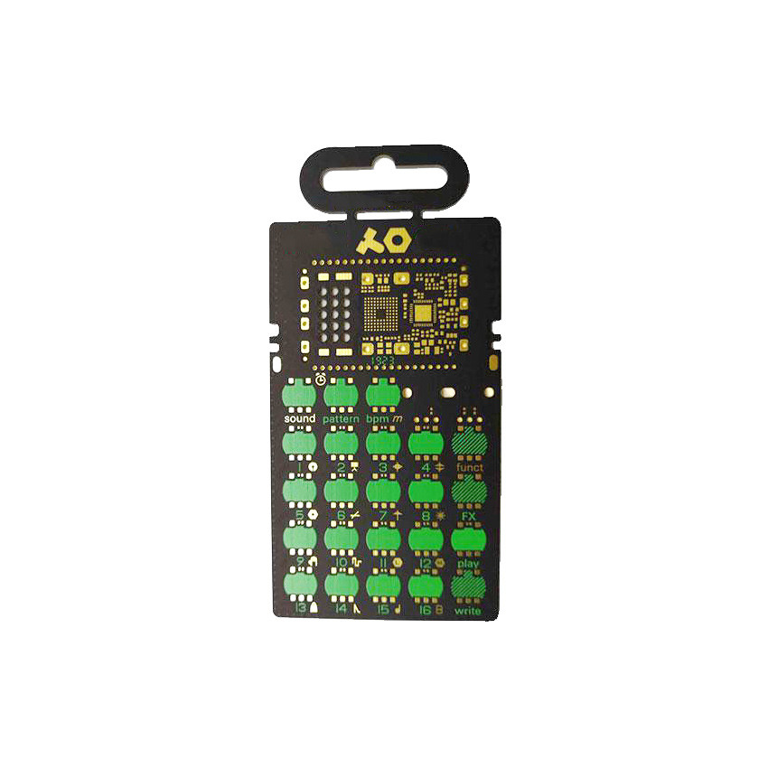
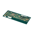
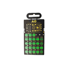
Differential Pair Altium Circuit Card Assy HDI PCB Solidworks Bom Template
Introduction to HDI
HDI (High Density Interconnect): High-density interconnection technology, mainly using micro-blind / buried vias (blind / buried vias), a technology that makes HDI PCB circuit board circuit distribution density higher. The advantage is that it can greatly increase the usable area of the PCB circuit board, making the product as miniaturized as possible. However, due to the increase in line distribution density, it is impossible to use traditional drilling methods to drill through holes, and some of the via holes must be drilled with laser drilling to form blind holes, or cooperate with inner-layer buried vias to interconnect.Generally speaking, HDI circuit boards use the build-up method (Build Up), first do or press the inner layers, laser drilling and electroplating on the outer layer are completed, and then the outer layer is covered with an insulating layer (prepreg). ) and copper foil, and then repeat the outer layer circuit making, or continue to laser drill, and stack the layers outward one at a time.
Generally, the diameter of the laser drilling hole is designed to be 3 ~ 4 mil (about 0.076 ~ 0.1 mm), and the insulation thickness between each laser drilling layer is about 3 mil. Due to the use of laser drilling many times, the key to the quality of the HDI circuit board is the hole pattern after laser drilling and whether the hole can be evenly filled after the subsequent electroplating and filling.
The following are examples of HDI PCB board types. The pink holes in the picture are blind holes, which are made by laser drilling, and the diameter is usually 3 to 4 mil; the yellow holes are buried holes, which are made by mechanical drilling, and the diameter is at least 6 mil (0.15 mm).
Medical equipment
Electronics make a major contribution to health - the nursing industry, as diagnostic, monitoring and therapeutic equipment. As the development of electronics becomes more efficient and dense, the medical applications of these electronic devices continue to grow, leading to endless new possibilities.At the heart of these medical devices is the HDI PCB. PCBs in the medical industry are highly specialized to accommodate the unique constraints of medical devices. In many medical applications, small packages are required to meet the size requirements for implants or emergency room monitors. Therefore, medical PCBs tend to be specialty high-density interconnect PCBs, also known as HDI PCBs. Medical PCBs can also be made with flexible substrates that allow the HDI PCB to bend during use, which is essential for both internal and external medical devices.
1. Monitors: Personal and healthcare monitors, including blood glucose monitors, heart rate and blood pressure monitors, and more.
2. Scanning Technology: CT scanners and ultrasound technology typically use PCB-based electronics.
3. Control System: The device controls the infusion, flow rate and distribution are electronically controlled.
4. Internal Devices: Pacemakers and similar internal medical devices keep patients healthy and are operated by a central micro-PCB.
PCB Capacities and Technical Specification
| NO. | Items | Capabilities |
| 1 | Layers | 2-68L |
| 2 | Maximum machining size | 600mm*1200mm |
| 3 | Board thickness | 0.2mm-6.5mm |
| 4 | Copper thickness | 0.5oz-28oz |
| 5 | Min trace/space | 2.0mil/2.0mil |
| 6 | Minimum finished aperture | 0. 10mm |
| 7 | Maximum thickness to diameter ratio | 15:1 |
| 8 | Via treatment | Via, blind&buried via, via in pad, Copper in via … |
| 9 | Surface finish/treatment | HASL/HASL lead free, Chemical tin, Chemical Gold, Immersion gold Inmersion Silver/Gold, Osp, Gold Plating |
| 10 | Base Material | FR408 FR408HR, PCL-370HR;IT180A, Megtron 6(Panasonic);Rogers4350, Rogers4003, RO3003, Rogers/Taconic/Arlon/Nelco laminate with FR-4 material(including partial Ro4350B hybrid laminating with FR-4) |
| 11 | Solder mask color | Green.Black.Red.Yellow.White.Blue.Purple.Matte Green. Matte Black |
| 12 | Testing Service | AOI, X-Ray, Flying-Probe, Function Test, First Article Tester |
| 13 | Profiling Punching | Routing,V-CUT,Beveling |
| 14 | Bow&twist | ≤0.5% |
| 15 | HDI type | 1+n+1,2+n+2,3+n+3 |
| 16 | Min mechanical aperture | 0.1mm |
| 17 | Min laser aperture | 0.075mm |
Company introduction
CESGATE is a company with a senior team. 80% of the senior management have a master's degree or above, and 100% of the sales team have a bachelor's degree or above. We operate 24 hours a day, 7 days a day, to provide customers with the best services and solutions. Our factory is located in Building 6, Fuyuan industrial park, Qiaotang road, Fuyong street , Shenzhen city, China , with a central warehouse of 1600 square meters, which can meet your production needs. With its own strength and professional ability, our group is your preferred electronic component distributor service.
![]()
![]()
![]()
![]()
![]()
![]()
![]()
FAQ
| Q: What is needed for PCB & PCBA quotation? CESGATE: For PCB: Gerber file and technic requirements(material,size, surface finish treatment, copper thickness,board thickness) and quantity you need. For PCBA: Files mentioned above, BOM, pick and place file. |
| Q: What is the difference between the HDI board and the general circuit board? CESGATE: Most of HDI use laser to form holes, while general circuit boards only use mechanical drilling, and HDI boards are manufactured by the build-up method (Build Up), so more layers will be added, while general circuit boards are only added once. |
| Q: What are the main products of your PCB/PCBA services? CESGATE: Automotive, Military, Aerospace, Industry Control, Medical care, IOT, Smart Home, Robot, Auto parts, Camera, UAV. |
| Q: What is your minimum order quantity (MOQ)? CESGATE: Our MOQ is 1 PCS, we are able to handle Small as well as large volume production with flexibility. |
| Q: The Wire Bonding process is required when the circuit board is printed. What should I pay attention to when making the circuit board? CESGATE: When making circuit boards, the surface treatment options are mostly "nickel palladium gold ENEPIG" or "chemical gold ENIG". If the Al aluminum wire is used, the gold thickness is recommended to be 3μ”~5μ”, but if the Au gold wire is used, the gold thickness should preferably be more than 5μ”. |