
| Place of Origin: | China |
|---|---|
| Brand Name: | CESGATE |
| Certification: | ISO9001/ ISO14001 |
| Model Number: | NA |
| Minimum Order Quantity: | 1PCS( NO MOQ) |
| Price: | Negotiable (Depends on your GERBER and BOM) |
| Packaging Details: | PCB: Vacuum Packing / PCBA: ESD Packing |
| Delivery Time: | 1-30 working days |
| Payment Terms: | T/T, L/C |
| Supply Ability: | 30,000pcs/month |
| Product Name: | Quick Turn Pcb Prototypes Multilayer PCB Circuit Board Soldering Pads Through Hole | Feature: | Soldering Through Hole |
|---|---|---|---|
| Supply Ability: | 1000 Unit/Units Per Week | Testing Service: | AOI X-Ray Function Test |
| Service: | Full Turnkey Service PCB+Components+Assembly | Function: | PCBA Board Service Prototype PCB Assembly |
| Board Thickness: | 1.6mm | Min Components Size: | 0201-54 Sq.mm (0.084 Sq.inch),Long Connector,CSP,BGA,QFP |
| High Light: | Hakko C1390c Multilayer PCB 1.6mm,Multilayer PCB Ipc2221 Bom Tally |
||
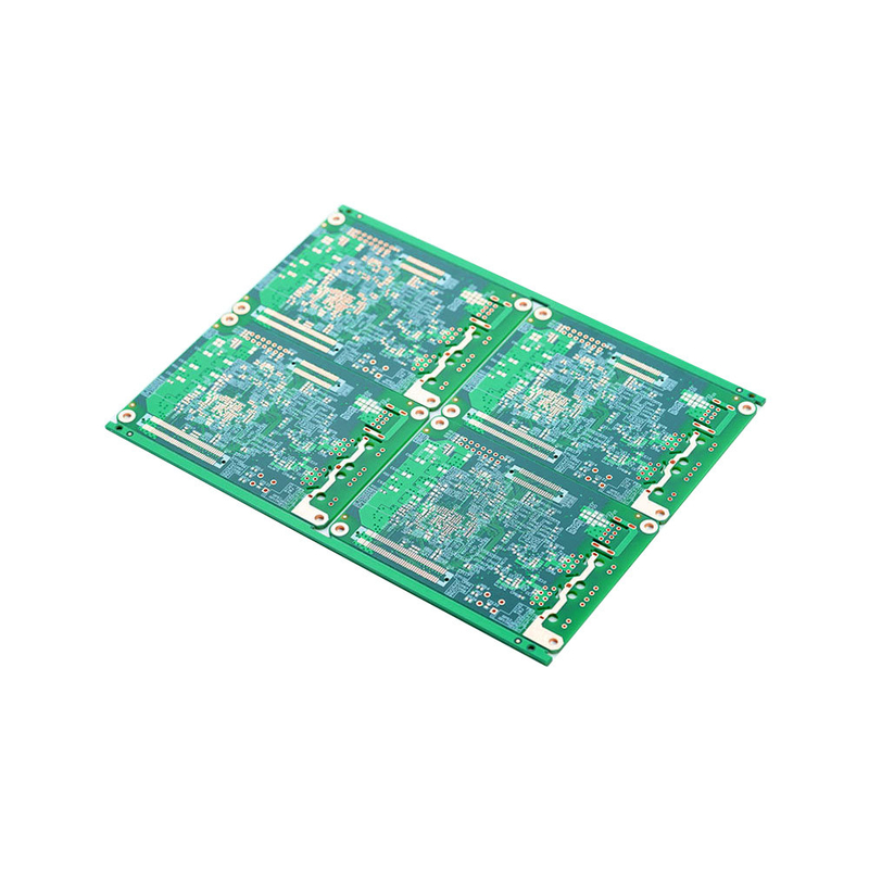
Quick Turn Pcb Prototypes Multilayer PCB Circuit Board Soldering Pads Through Hole
Lead-time for multilayer PCB Components Sourcing
This is the duration required to manufacture a component. It includes order preparation, queue, setup, run, inspection and put-away time.
For products made on an order, it’s the time taken from the release of an order, to production and shipment.
Escalating lead time is one of the emerging trends in Electronic component sourcing. This creates a big challenge for purchasing communities.
There is usually no stability when it comes to lead times.
Escalating lead times is a complicated situation rising due to market demands, investment constraints and capacity allocations in some regions.
Lead-time usually is between 5- 8 working days from the initial day of order. For mass production lead time can take up to 2 weeks.
However, this may differ from one region to the other. For example, Lead times for resistors in North America had moved from 12 to 16 weeks by the beginning of 2017.
PCB Capabilities
| NO. | Items | Capabilities |
| 1 | Layers | 2-68L |
| 2 | Maximum machining size | 600mm*1200mm |
| 3 | Board thickness | 0.2mm-6.5mm |
| 4 | Copper thickness | 0.5oz-28oz |
| 5 | Min trace/space | 2.0mil/2.0mil |
| 6 | Minimum finished aperture | 0. 10mm |
| 7 | Maximum thickness to diameter ratio | 15:1 |
| 8 | Via treatment | Via, blind&buried via, via in pad, Copper in via … |
| 9 | Surface finish/treatment | HASL/HASL lead free, Chemical tin, Chemical Gold, Immersion gold Inmersion Silver/Gold, Osp, Gold Plating |
| 10 | Base Material | FR408 FR408HR, PCL-370HR;IT180A, Megtron 6(Panasonic);Rogers4350, Rogers4003, RO3003, Rogers/Taconic/Arlon/Nelco laminate with FR-4 material(including partial Ro4350B hybrid laminating with FR-4) |
| 11 | Solder mask color | Green.Black.Red.Yellow.White.Blue.Purple.Matte Green. Matte Black |
| 12 | Testing Service | AOI, X-Ray, Flying-Probe, Function Test, First Article Tester |
| 13 | Profiling Punching | Routing,V-CUT,Beveling |
| 14 | Bow&twist | ≤0.5% |
| 15 | HDI type | 1+n+1,2+n+2,3+n+3 |
| 16 | Min mechanical aperture | 0.1mm |
| 17 | Min laser aperture | 0.075mm |
Who are we?
In business since 2010, CESGATE mainly provides pcb fabrication and design service for customers from all over the world. We have ISO and UL certificate,and honored as HI-TECH enterprise by Chengdu goverment.
As a professional multilayer PCB factory , we can provide prototype and low-to-mid volume multilayer PCB fabrication and design services for our customers. We are in Chengdu, China, which is the largest center of technology and electronics manufacturing in the world. Cooperating with our engineering team, quality team, these allow us to offer our customers low-cost, One-stop PCB Services.
![]()
![]()
![]()
![]()
![]()
![]()
![]()
FAQ
| Q: What is the difference between the HDI board and the general circuit board? CESGATE: Most of HDI use laser to form holes, while general circuit boards only use mechanical drilling, and HDI boards are manufactured by the build-up method (Build Up), so more layers will be added, while general circuit boards are only added once. |
| Q: What does CESGATE need for a customized PCB order? CESGATE: When you place a PCB order, the customers need to provide Gerber or pcb file. If you do not have the file in the correct format, you can send all the details related to the products. |
| Q: Do you have any other services? CESGATE: We mainly focus on the procurement services of PCB + assembly + components. In addition, we can also provide programming, testing, cable, housing assembly services. |
| Q: The Wire Bonding process is required when the circuit board is printed. What should I pay attention to when making the circuit board? CESGATE: When making circuit boards, the surface treatment options are mostly "nickel palladium gold ENEPIG" or "chemical gold ENIG". If the Al aluminum wire is used, the gold thickness is recommended to be 3μ”~5μ”, but if the Au gold wire is used, the gold thickness should preferably be more than 5μ”. |