| Place of Origin: | China |
|---|---|
| Brand Name: | CESGATE |
| Certification: | ISO9001/ ISO14001 |
| Model Number: | NA |
| Minimum Order Quantity: | 1PCS( NO MOQ) |
| Price: | Negotiable (Depends on your GERBER and BOM) |
| Packaging Details: | PCB: Vacuum Packing / PCBA: ESD Packing |
| Delivery Time: | 1-30 working days |
| Payment Terms: | T/T, L/C |
| Supply Ability: | 30,000pcs/month |
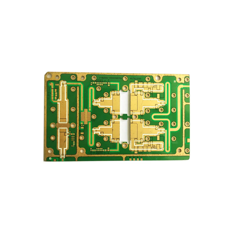
| Product Name: | 2 Oz Copper Pcb High Frequency PCB 94v 0 Circuit Board Pcb Material Fr4 | Feature: | 2 Oz Copper Pcb |
|---|---|---|---|
| Min. Line Width: | 0.2mm, 3mi, 0.075mm, 0.075mm/0.075mm(3mil/3mil), 0.1 0mm | Sub-assembly: | Plastic,metal,screen |
| Min Trace/gap: | 0.075mm Or 3mil | Copper Thickness: | 1oz, 1/2OZ 1OZ 2OZ 3OZ, As Your Request, 0.5-3.0 Oz, 1 Oz |
| Base Material: | FR4, Aluminum, Rogers, TG | Surface Finishing: | HASL, OSP, ENIG, Immersion Gold, HASL Lead Free/OSP/Soft Gold/Hard Gold |
| High Light: | 2Oz Copper High Frequency PCB,94v 0 Circuit Board Pcb,Fr4 High Frequency PCB |
||
2 Oz Copper Pcb High Frequency PCB 94v 0 Circuit Board Pcb Material Fr4
Characteristics of High Frequency PCB Laminate Material
Understanding the characteristics of your High Frequency PCB laminate material is critical when manufacturing your PCB.
Dielectric constant (Er)
You will be able to identify and understand the behavior of your PCB.
Dielectric constant is a measure of the ability of a material to store electrical energy while in an electric field.
This ability depends on the direction of the current implying that the dielectric current changes as the axis of the material changes.
What you need to understand is the frequency range that you will subject the material to while testing.
Also, you need to know the testing method and any variable present for the frequency range.
Lastly, you have to consider the constant dielectric conditions of your PCB that can match that of your application.
High Frequency PCB Fabrication Process
Design your PCB
The starting point in the manufacturing of your PCB is to have a design for the PCB. This involves having a plan where you will lay the blueprint for your PCB.
The most common designer software that uses for your PCB is the Extended Gerber.
Extended Gerber will assist you in encoding the relevant information that you may need.
This information includes the number of layers of your copper and the number of solder masks that you will need.
When you have encoded your PCB blueprint using the Gerber Extended Software, you need to confirm other aspects of your design.
After finishing all these, you will have to take your design to the fabrication center where manufacturing will take place.
It is here where your design will undergo a DFM check to ensure that your design attains the tolerance that meets the requirements is for production.
PCB Capacities and Technical Specification
| NO. | Items | Capabilities |
| 1 | Layers | 2-68L |
| 2 | Maximum machining size | 600mm*1200mm |
| 3 | Board thickness | 0.2mm-6.5mm |
| 4 | Copper thickness | 0.5oz-28oz |
| 5 | Min trace/space | 2.0mil/2.0mil |
| 6 | Minimum finished aperture | 0. 10mm |
| 7 | Maximum thickness to diameter ratio | 15:1 |
| 8 | Via treatment | Via, blind&buried via, via in pad, Copper in via … |
| 9 | Surface finish/treatment | HASL/HASL lead free, Chemical tin, Chemical Gold, Immersion gold Inmersion Silver/Gold, Osp, Gold Plating |
| 10 | Base Material | FR408 FR408HR, PCL-370HR;IT180A, Megtron 6(Panasonic);Rogers4350, Rogers4003, RO3003, Rogers/Taconic/Arlon/Nelco laminate with FR-4 material(including partial Ro4350B hybrid laminating with FR-4) |
| 11 | Solder mask color | Green.Black.Red.Yellow.White.Blue.Purple.Matte Green. Matte Black |
| 12 | Testing Service | AOI, X-Ray, Flying-Probe, Function Test, First Article Tester |
| 13 | Profiling Punching | Routing,V-CUT,Beveling |
| 14 | Bow&twist | ≤0.5% |
| 15 | HDI type | 1+n+1,2+n+2,3+n+3 |
| 16 | Min mechanical aperture | 0.1mm |
| 17 | Min laser aperture | 0.075mm |
Company Profile
CESGATE is a company with a senior team. 80% of the senior management have a master's degree or above, and 100% of the sales team have a bachelor's degree or above. We operate 24 hours a day, 7 days a day, to provide customers with the best services and solutions. Our factory is located in Building 6, Fuyuan industrial park, Qiaotang road, Fuyong street , Shenzhen city, China , with a central warehouse of 1600 square meters, which can meet your production needs. With its own strength and professional ability, our group is your preferred electronic component distributor service.
![]()
![]()
![]()
![]()
![]()
![]()
![]()
FAQ
| Q: What modes of transport are there? CESGATE: Usually includes express, air shipment, rail shipment and sea shipment. |
| Q: Popular field? CESGATE: Semiconductor, Smart Home, Medical Products, Smart Wearable, Industrial Control, IOT etc. |
| Q: Can you give us a preferential discount? CESGATE: Of course, we will offer a preferential discount for your large orders and confirm the order quickly. |
| Q: Why choose us? CESGATE: Professional and experienced R&D team. Advanced production equipment, scientific and reasonable process flow. Reliable and strict quality control system. We test all our products before shipment to make sure everything is in perfect condition. |
| Q: How long does it take for PCB quote? CESGATE: Normally 12 hours to 48 hours as soon as receive internal engineer evaluate confirmation. |