
| Place of Origin: | China |
|---|---|
| Brand Name: | CESGATE |
| Certification: | ISO9001/ ISO14001 |
| Model Number: | NA |
| Minimum Order Quantity: | 1PCS( NO MOQ) |
| Price: | Negotiable (Depends on your GERBER and BOM) |
| Packaging Details: | PCB: Vacuum Packing / PCBA: ESD Packing |
| Delivery Time: | 1-30 working days |
| Payment Terms: | T/T, L/C |
| Supply Ability: | 30,000pcs/month |
| Product Name: | CEM3 Materials BOM Sourcing OEM Stack Up High Frequency PCB Rogers 4350 | Feature: | BOM Sourcing |
|---|---|---|---|
| Function Test: | 100% Functional Test | Min. Hole Size: | 0.20mm, 0.1mm, 8 Mil, 0.254-0.40mm, 0.1mm-1mm |
| Surface Finishing: | HASL, OSP, ENIG, Immersion Gold, HASL Lead Free/OSP/Soft Gold/Hard Gold | Testing Service: | AOI X-Ray Function Test |
| Silkscreen Color: | White, White Or On Your Request., Black, Green/white/yellow/black/blue/purple | Base Material: | RO3003, RO4350, PTFE, TU872, M4, M6 |
| High Light: | High Frequency PCB Rogers 4350,pcb prototype board Rogers 4350,Shengyi pcb prototype board |
||
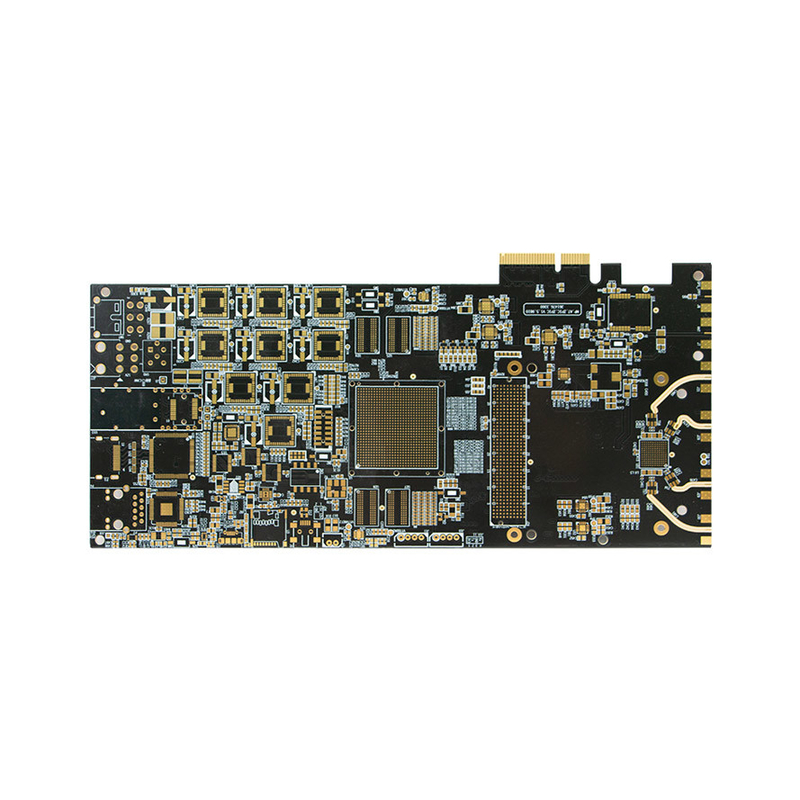
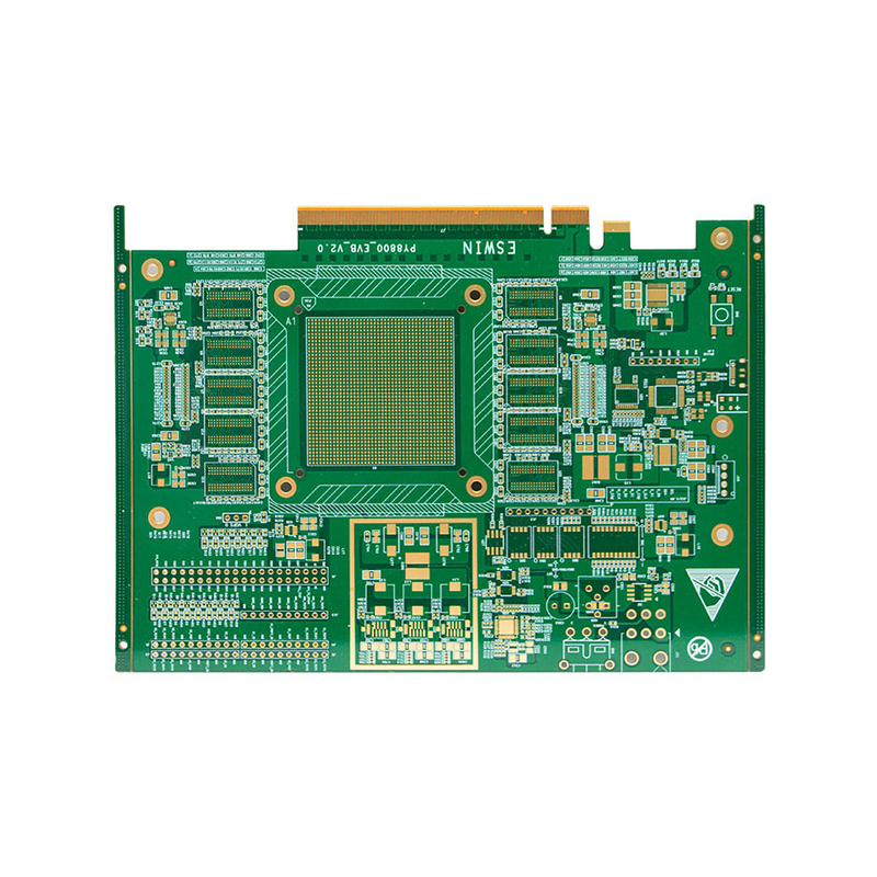
CEM3 Materials BOM Sourcing OEM Stack Up High Frequency PCB Rogers 4350
Your Expert High Frequency PCB manufacturer
According to ITU (The International Telecommunication Union)designation)designation, the High frequency (HF) is the range of radio frequency electromagnetic waves (radio waves) between 3 and 30 megahertz (MHz).
In PCB industry, however, we consider any high frequency PCBs that operates above 100MHz as High Frequency (HF) PCB.
The laminate materials for building high frequency PCB are with very specific characteristics, such as dielectric constant (Er), loss tangent, and CTE (co-efficient of thermal expansion), these laminates have more advanced composites compare to normal FR-4 material
High frequency PCBs were firstly used in military applications, and then become more and more popular in medical application such as wireless hand held equipment, and then in nowadays industrial applications such as advanced communications systems for base stations, radar, and global positioning products.
High Frequency PCB Fabrication Process
Lamination of the PCB layers
Once your PCB is free of errors, you can now move to the next step of the manufacturing process. During lamination, fusing of the layers of your PCB takes place.
The main steps that take place here are laminating PCB and lay- up steps. The outer part of your PCB consists of fiberglass precoated using epoxy resin.
A thin layer of copper foil covers the original material for your PCB with copper engravings.
After preparing the inner and outer layer of your PCB, you can go ahead and join them together.
You can use a metal clamp and a particular press table to sandwich the layers.
Fitting of the layers onto the table is by using a unique pin.
You can start this process by placing a pre-coated epoxy resin layer on the alignment bottom of the table.
You then place a layer of substrate on top of the resin layer and then a copper foil layer.
On top of the copper foil, you will add layers of pre-impregnated resins and then another copper foil layer.
Lastly, you will place a piece of press plate.
After that, you can now press the layers. You can use pins to punch down through the layers which ensure that you have fixed the layers correctly.
The next step is to laminate the PCB. Here, a pair of heated plate transfers heat and pressure to the PCB layers.
The heat will melt the epoxy while the pressure fuses the layers.
You will have to unpack the top press and the pins which will allow the actual PCB to be free.
PCB Capacities and Technical Specification
| NO. | Items | Capabilities |
| 1 | Layers | 2-68L |
| 2 | Maximum machining size | 600mm*1200mm |
| 3 | Board thickness | 0.2mm-6.5mm |
| 4 | Copper thickness | 0.5oz-28oz |
| 5 | Min trace/space | 2.0mil/2.0mil |
| 6 | Minimum finished aperture | 0. 10mm |
| 7 | Maximum thickness to diameter ratio | 15:1 |
| 8 | Via treatment | Via, blind&buried via, via in pad, Copper in via … |
| 9 | Surface finish/treatment | HASL/HASL lead free, Chemical tin, Chemical Gold, Immersion gold Inmersion Silver/Gold, Osp, Gold Plating |
| 10 | Base Material | FR408 FR408HR, PCL-370HR;IT180A, Megtron 6(Panasonic);Rogers4350, Rogers4003, RO3003, Rogers/Taconic/Arlon/Nelco laminate with FR-4 material(including partial Ro4350B hybrid laminating with FR-4) |
| 11 | Solder mask color | Green.Black.Red.Yellow.White.Blue.Purple.Matte Green. Matte Black |
| 12 | Testing Service | AOI, X-Ray, Flying-Probe, Function Test, First Article Tester |
| 13 | Profiling Punching | Routing,V-CUT,Beveling |
| 14 | Bow&twist | ≤0.5% |
| 15 | HDI type | 1+n+1,2+n+2,3+n+3 |
| 16 | Min mechanical aperture | 0.1mm |
| 17 | Min laser aperture | 0.075mm |
CESGATE's Advantages
Test each function of the product according to the test case, and provide the test report. We can provide services such as electrical measurement and aging according to customer needs to improve product reliability.
For each process, CESGATE has formulated perfect operation instructions, and customized targeted inspection standards according to products in different industries, so as to improve the pass-through rate of products from each link.
![]()
![]()
![]()
![]()
![]()
![]()
![]()
FAQ
| Q: Why choose us? CESGATE: Professional and experienced R&D team. Advanced production equipment, scientific and reasonable process flow. Reliable and strict quality control system. We test all our products before shipment to make sure everything is in perfect condition. |
| Q: How long does it take for PCB quote? CESGATE: Normally 12 hours to 48 hours as soon as receive internal engineer evaluate confirmation. |
| Q: The Wire Bonding process is required when the circuit board is printed. What should I pay attention to when making the circuit board? CESGATE: When making circuit boards, the surface treatment options are mostly "nickel palladium gold ENEPIG" or "chemical gold ENIG". If the Al aluminum wire is used, the gold thickness is recommended to be 3μ”~5μ”, but if the Au gold wire is used, the gold thickness should preferably be more than 5μ”. |