
| Place of Origin: | China |
|---|---|
| Brand Name: | CESGATE |
| Certification: | ISO9001/ ISO14001 |
| Model Number: | NA |
| Minimum Order Quantity: | 1PCS( NO MOQ) |
| Price: | Negotiable (Depends on your GERBER and BOM) |
| Packaging Details: | PCB: Vacuum Packing / PCBA: ESD Packing |
| Delivery Time: | 1-30 working days |
| Payment Terms: | T/T, L/C |
| Supply Ability: | 30,000pcs/month |
| Product Name: | AOI Testing Fast Delivery Ki-CAD High Frequency PCB Taconic High Spped Voltage | Feature: | High Spped Voltage |
|---|---|---|---|
| Min. Line Width: | 0.2mm, 3mi, 0.075mm, 0.075mm/0.075mm(3mil/3mil), 0.1 0mm | Min. Hole Size: | 0.20mm, 0.1mm, 8 Mil, 0.254-0.40mm, 0.1mm-1mm |
| Surface Finishing: | HASL, OSP, ENIG, Immersion Gold, HASL Lead Free/OSP/Soft Gold/Hard Gold | Service: | Competitive Price, PCB/Components Sourcing/Soldering/Progamming/Testing.., PCB&PCBA, Professional Engineer, EMS/OMD/OEM/turnkey Assembly |
| Silkscreen Color: | White, White Or On Your Request., Black, Green/white/yellow/black/blue/purple | Base Material: | RO3003, RO4350, PTFE, TU872, M4, M6 |
| High Light: | Ki-CAD high speed pcb,Ki-CAD High Frequency PCB,high speed pcb 600mm*1200mm |
||
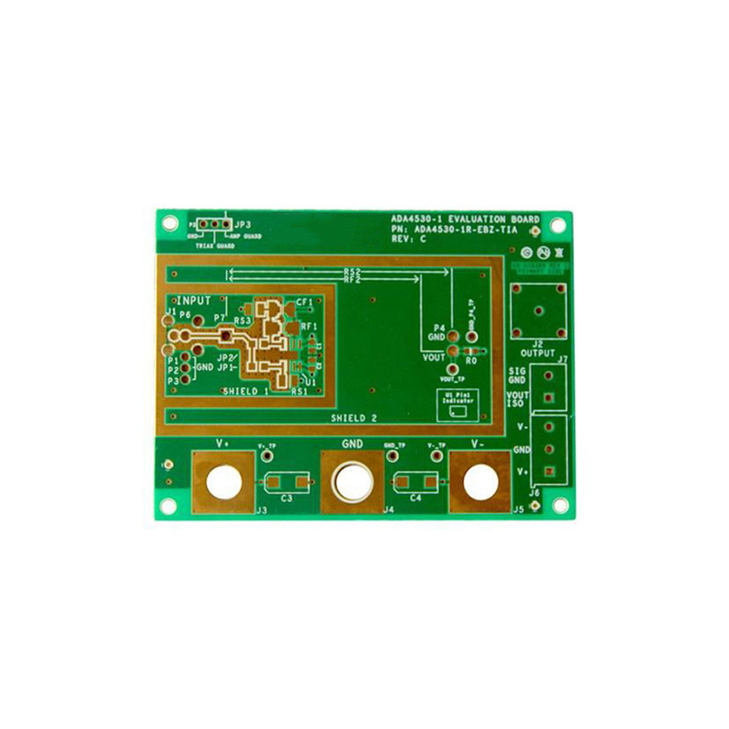
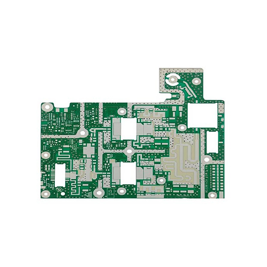
AOI Testing Fast Delivery Ki-CAD High Frequency PCB Taconic High Spped Voltage
How to Choose Best Material for High Frequency PCB
Having the right material for your High Frequency PCB will minimize the chances of your circuit by sending mixed signals.
By having materials, such that have suboptimal copper foil can have severe effects on your circuit.
That is why you need to select the correct High Frequency PCB material for your circuit.
Consider Top High Frequency PCB Material Manufacturers
Several companies manufacture High Frequency PCBs. However, not all of them meet the standards international standards. Always ensure that you obtain your PCB materials from the best manufacturers. Among the top manufacturers that you can source for your PCB materials include the following.
You can choose Polyclad
If you are looking for a company that offers high-quality PCB materials, then you can pick Polyclad.
There are a variety of materials that they provide such as copper foil, solder masks, and boards.
Polyclad also offers assistance in designing and manufacturing your PCB.
There is a guarantee that you will get service on the materials that you purchase at Polyclad.
High Frequency PCB Fabrication Process
Evaluate Dielectric Constant
You will have to take into consideration the dielectric constant of the PCB substrate.
Dielectric constant refers to the ability of a PCB material to retain energy in the electric field.
This will depend on which direction the material takes. As such, an effective dielectric constant need to be very small to deliver a stable input.
It is this input that will help minimize delay in the transmission of signals.
What you need to note is that the constant dielectric substrate needs to match for your PCB to function correctly.
If you have constant dielectric substrates that are not uniform may create problems in the functioning of your PCB.
Among the constant dielectric substrate that you can have include resins and woven materials.
PCB Capacities and Technical Specification
| NO. | Items | Capabilities |
| 1 | Layers | 2-68L |
| 2 | Maximum machining size | 600mm*1200mm |
| 3 | Board thickness | 0.2mm-6.5mm |
| 4 | Copper thickness | 0.5oz-28oz |
| 5 | Min trace/space | 2.0mil/2.0mil |
| 6 | Minimum finished aperture | 0. 10mm |
| 7 | Maximum thickness to diameter ratio | 15:1 |
| 8 | Via treatment | Via, blind&buried via, via in pad, Copper in via … |
| 9 | Surface finish/treatment | HASL/HASL lead free, Chemical tin, Chemical Gold, Immersion gold Inmersion Silver/Gold, Osp, Gold Plating |
| 10 | Base Material | FR408 FR408HR, PCL-370HR;IT180A, Megtron 6(Panasonic);Rogers4350, Rogers4003, RO3003, Rogers/Taconic/Arlon/Nelco laminate with FR-4 material(including partial Ro4350B hybrid laminating with FR-4) |
| 11 | Solder mask color | Green.Black.Red.Yellow.White.Blue.Purple.Matte Green. Matte Black |
| 12 | Testing Service | AOI, X-Ray, Flying-Probe, Function Test, First Article Tester |
| 13 | Profiling Punching | Routing,V-CUT,Beveling |
| 14 | Bow&twist | ≤0.5% |
| 15 | HDI type | 1+n+1,2+n+2,3+n+3 |
| 16 | Min mechanical aperture | 0.1mm |
| 17 | Min laser aperture | 0.075mm |
Company Introduction
CESGATE provides Electronic Manufacturing Services (EMS) for your products that require surface mount, through hole, BGA and mixed technology.
Our main services include PCB assembly (Electronic assembly), component procurement and PCB fabrication from quick turn, sample run to volume production.
Our customers are who of the Medical, Instrumentation, Intelligent home, Automotive, Consumer electronics industry and Robotics industries.
Full range of PCB manufacturing and assembly services to fit all of your printed circuit board needs.
![]()
![]()
![]()
![]()
![]()
![]()
![]()
FAQ
| Q: HOW DO YOU MAKE OUR BUSINESS LONG-TERM AND GOOD RELATIONSHIP? CESGATE: 1. We would like to offer sample if the buyer really want to make long-term relationship with us. 2. We keep good quality and competitive price to ensure our customers benefit. 3. We respect customers as our friend and sincerely do business and make friends with them,no matter where they come from. |
| Q: Do you support fast proofing? CESGATE: Yes, we support fast proofing within 3-7 days. |
| Q: Are my files safe? CEGSATE: Your files are kept very safe, and we are protecting intellectual property for our clients throughout the process. All files provided by customers are never shared with any third party. |
| Q: MOQ? CESGATE: There is no MOQ in POE. We are able to flexibly handle small and large batches. |