| Place of Origin: | China |
|---|---|
| Brand Name: | CESGATE |
| Certification: | ISO9001/ ISO14001 |
| Model Number: | NA |
| Minimum Order Quantity: | 1PCS( NO MOQ) |
| Price: | Negotiable (Depends on your GERBER and BOM) |
| Packaging Details: | PCB: Vacuum Packing / PCBA: ESD Packing |
| Delivery Time: | 1-30 working days |
| Payment Terms: | T/T, L/C |
| Supply Ability: | 30,000pcs/month |
| Product Name: | Turnkey Services Rogers Schematic Thin Soldering High Frequency PCB Stack Up | Feature: | Schematic |
|---|---|---|---|
| Min. Line Width: | 0.2mm, 3mi, 0.075mm, 0.075mm/0.075mm(3mil/3mil), 0.1 0mm | Min. Hole Size: | 0.20mm, 0.1mm, 8 Mil, 0.254-0.40mm, 0.1mm-1mm |
| Surface Finishing: | HASL, OSP, ENIG, Immersion Gold, HASL Lead Free/OSP/Soft Gold/Hard Gold | Solder Mask: | White, Blue, Green. Red. Blue. White. Black.Yellow, Green, Black |
| Copper Thickness: | 1oz, 1/2OZ 1OZ 2OZ 3OZ, As Your Request, 0.5-3.0 Oz, 1 Oz | Base Material: | FR4, Aluminum, Rogers, CEM-1, TG |
| High Light: | Tin Soldering turnkey pcb,Tin Soldering green pcb board,green pcb board ENIG Immersion Gold |
||
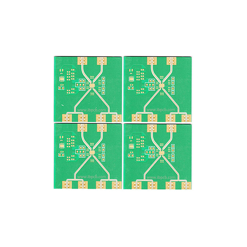
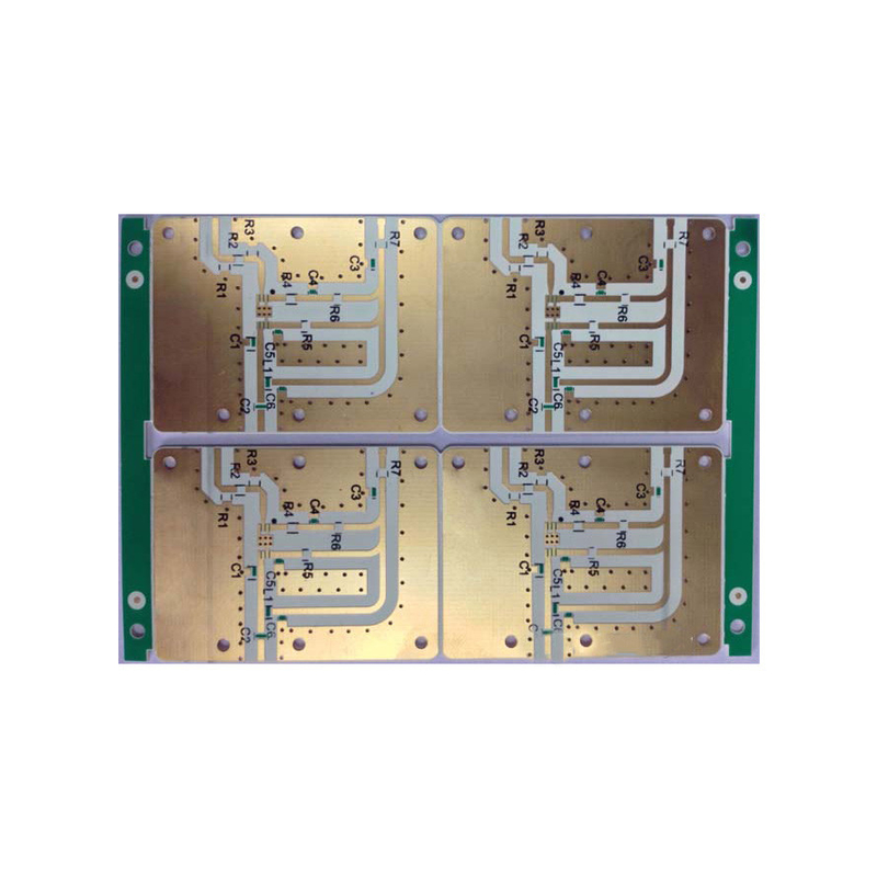
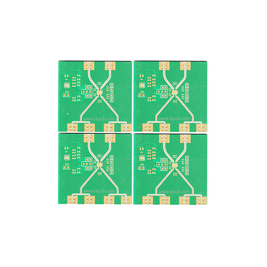
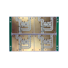
Turnkey Services Rogers Schematic Thin Soldering High Frequency PCB Stack Up
High Frequency PCB Fabrication Process
Imaging and plating of the outer layer
This process involves applying to resist the outer layer through imaging.
After coating and imaging of the outer layer, you have to plate the interior layer in the same way as previously.
At this stage, the plating of the outer layer aids in protecting the copper on the outer side.
Document all Your Board Stack Up Plan for Manufacturing
Once you have a plan of how you are going to design your PCB, you will have to document the requirements for your stack up layer.
You can consult with your manufacturer to determine the specifics for your PCBs.
This includes understanding the materials and the specific constraints for your PCB. You can either use FR-4, Nelco or Rodgers materials for your PCB.
You can have other strategies for your stack up such as having a signal layer which you can place next on an adjacent layer. This will offer signals that have an efficient return path.
You can also consider routing the High Frequency PCB signals which are on the inner layers of your PCB between planes.
This will offer to shield over any radiation that it emits externally.
Also, on your layer stack up, you may use many ground planes.
The purpose for this is to reduce your reference hinderance which in turn minimizes the effect of radiation on your circuit.
What is the difference between high speed PCB and high frequency PCB?
High speed and high frequency pcb is different. High-speed circuit refers to that the voltage rises or falls in a short period of time, and High Frequency circuit refers to that the circuit has a short period. But there is no exact difference between a high-speed PCB and a High Frequency PCB. Even the basic materials are the same. So if you ask the difference between high-speed PCB and High Frequency PCB, ignore the name of the circuit board, and focus on how to maintain the signal integrity of the circuit.
PCB Capacities and Technical Specification
| NO. | Items | Capabilities |
| 1 | Layers | 2-68L |
| 2 | Maximum machining size | 600mm*1200mm |
| 3 | Board thickness | 0.2mm-6.5mm |
| 4 | Copper thickness | 0.5oz-28oz |
| 5 | Min trace/space | 2.0mil/2.0mil |
| 6 | Minimum finished aperture | 0. 10mm |
| 7 | Maximum thickness to diameter ratio | 15:1 |
| 8 | Via treatment | Via, blind&buried via, via in pad, Copper in via … |
| 9 | Surface finish/treatment | HASL/HASL lead free, Chemical tin, Chemical Gold, Immersion gold Inmersion Silver/Gold, Osp, Gold Plating |
| 10 | Base Material | FR408 FR408HR, PCL-370HR;IT180A, Megtron 6(Panasonic);Rogers4350, Rogers4003, RO3003, Rogers/Taconic/Arlon/Nelco laminate with FR-4 material(including partial Ro4350B hybrid laminating with FR-4) |
| 11 | Solder mask color | Green.Black.Red.Yellow.White.Blue.Purple.Matte Green. Matte Black |
| 12 | Testing Service | AOI, X-Ray, Flying-Probe, Function Test, First Article Tester |
| 13 | Profiling Punching | Routing,V-CUT,Beveling |
| 14 | Bow&twist | ≤0.5% |
| 15 | HDI type | 1+n+1,2+n+2,3+n+3 |
| 16 | Min mechanical aperture | 0.1mm |
| 17 | Min laser aperture | 0.075mm |
Company introduction
Chengdu Cesgate Technology Co.,Ltd was found in Chengdu, China.The company is strong and professional technical, with perfect quality assurance system and advances test-analyzed instrument. CESGATE is one of the Professional PCB manufacturer from China. We have professional PCB designer for your PCB layout requirement. We design single, double, and multi layers , Rigid, flexible, Flex-Rigid printed circuit boards, and PCB assembly.
![]()
![]()
![]()
![]()
![]()
![]()
![]()
FAQ
| Q: What modes of transport are there? CESGATE: Usually includes express, air shipment, rail shipment and sea shipment. |
| Q: Popular field? CESGATE: Semiconductor, Smart Home, Medical Products, Smart Wearable, Industrial Control, IOT etc. |
| Q: Can you give us a preferential discount? CESGATE: Of course, we will offer a preferential discount for your large orders and confirm the order quickly. |
| Q: Why choose us? CESGATE: Professional and experienced R&D team. Advanced production equipment, scientific and reasonable process flow. Reliable and strict quality control system. We test all our products before shipment to make sure everything is in perfect condition. |