| Place of Origin: | China |
|---|---|
| Brand Name: | CESGATE |
| Certification: | UL、IATF16949、ISO9001 |
| Model Number: | N/A |
| Minimum Order Quantity: | 1PCS( NO MOQ) |
| Price: | Negotiable (Depends on your GERBER and BOM) |
| Packaging Details: | PCB: Vacuum Packing / PCBA: ESD Packing |
| Delivery Time: | 1-30 working days |
| Payment Terms: | T/T, L/C |
| Supply Ability: | 30,000pcs/month |
| Product Name: | FR4 Megtron 6 HASL Manufacturing Process Semiconductor PCB Fabrication Services | Feature: | Megtron 6 |
|---|---|---|---|
| Base Material: | FR-4, TACONIC, Aluminum, CEM-3, Metal/ceramic/aluminum Base | Type: | Semiconductor Tools Systems And Components, Equipment Comp |
| Solder Mask: | Green, White Black Green Blue Red, Green Or Other Color As You Want, Green/blue, Green Black Bule White | Application: | Electronics Device, Consumer Electronics, Communications, And So On, Universal |
| Solder Mask Color: | Green, Blue, White And Red, White Black Yellow Green Red, Purple | Testing Service: | Function Test, 100% Test |
| High Light: | Megtron 6 FR4 PCB Board,FR4 PCB Board Routing V CUT,Megtron 6 FR4 prototype pcb fabrication |
||
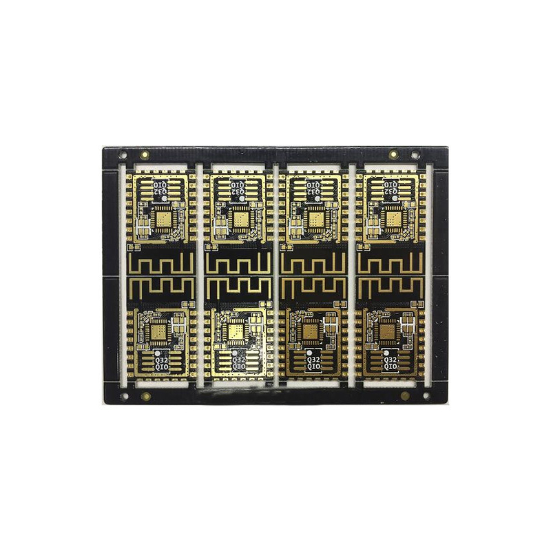
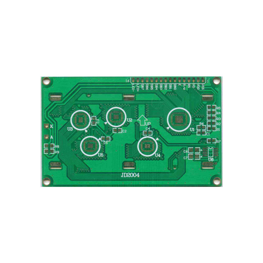
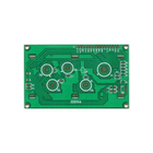
FR4 Megtron 6 HASL Manufacturing Process Semiconductor PCB Fabrication Services
Finding Solutions to the Semiconductor Supply Chain Problem
The best way to work around the semiconductor shortage is to partner with someone who has a lot of experience working with the component supply chain, like CESGATE. The component engineers and procurement specialists at a semiconductor PCB contract manufacturer have the necessary skill set for this job. They can bring the following assets to the table when the time comes to purchase parts for your next semiconductor PCB build:
Application
Validation Boards
Semiconductor PCB development is typically performed to create a prototype that may take several paths for production and application. Prototyping can be thought of as the creation of several board stages. One of the most important of these post-silicon stages is validation, which tests the full functionality of the semiconductor and demands
PCB Capacities and Technical Specification
| NO. | Items | Capabilities |
| 1 | Layers | 2-68L |
| 2 | Maximum machining size | 600mm*1200mm |
| 3 | Board thickness | 0.2mm-6.5mm |
| 4 | Copper thickness | 0.5oz-28oz |
| 5 | Min trace/space | 2.0mil/2.0mil |
| 6 | Minimum finished aperture | 0. 10mm |
| 7 | Maximum thickness to diameter ratio | 15:1 |
| 8 | Via treatment | Via, blind&buried via, via in pad, Copper in via … |
| 9 | Surface finish/treatment | HASL/HASL lead free, Chemical tin, Chemical Gold, Immersion gold Inmersion Silver/Gold, Osp, Gold Plating |
| 10 | Base Material | FR408 FR408HR, PCL-370HR;IT180A, Megtron 6(Panasonic);Rogers4350, Rogers4003, RO3003, Rogers/Taconic/Arlon/Nelco laminate with FR-4 material(including partial Ro4350B hybrid laminating with FR-4) |
| 11 | Solder mask color | Green.Black.Red.Yellow.White.Blue.Purple.Matte Green. Matte Black |
| 12 | Testing Service | AOI, X-Ray, Flying-Probe, Function Test, First Article Tester |
| 13 | Profiling Punching | Routing,V-CUT,Beveling |
| 14 | Bow&twist | ≤0.5% |
| 15 | HDI type | 1+n+1,2+n+2,3+n+3 |
| 16 | Min mechanical aperture | 0.1mm |
| 17 | Min laser aperture | 0.075mm |
Who are we?
![]()
![]()
![]()
![]()
![]()
![]()
![]()
FAQ
| Q: What is your delivery date? CESGATE: The general sample delivery time is 6 working days for single and double-sided boards, 7 working days for 4-layer boards, and an additional working day for every 2 layers. However, if there are special processes, additional working days will be added according to the situation. Generally, the delivery time for mass production is 10 working days for single and double-sided panels, and 15 working days for multi-layer panels. However, if there is a special process or more than a certain number of working days, the working days will be additionally increased according to the situation; you can also pay the urgent fee to shorten the number of days, please contact Contact the business specially proposed, depending on the individual situation to provide expedited days. |
| Q: What is the difference between the HDI board and the general circuit board? CESGATE: Most of HDI use laser to form holes, while general circuit boards only use mechanical drilling, and HDI boards are manufactured by the build-up method (Build Up), so more layers will be added, while general circuit boards are only added once. |
| Q: What are the types of solder mask? CESGATE: There are traditional epoxy resin IR baking type, UV curing type, Liquid Photo Imageable Solder Mask and Dry film solder mask. Currently, the liquid solder mask is the main type. |