
| Place of Origin: | China |
|---|---|
| Brand Name: | CESGATE |
| Certification: | ISO9001/ ISO14001 |
| Model Number: | NA |
| Minimum Order Quantity: | 1PCS( NO MOQ) |
| Price: | Negotiable (Depends on your GERBER and BOM) |
| Packaging Details: | PCB: Vacuum Packing / PCBA: ESD Packing |
| Delivery Time: | 1-30 working days |
| Payment Terms: | T/T, L/C |
| Supply Ability: | 30,000pcs/month |
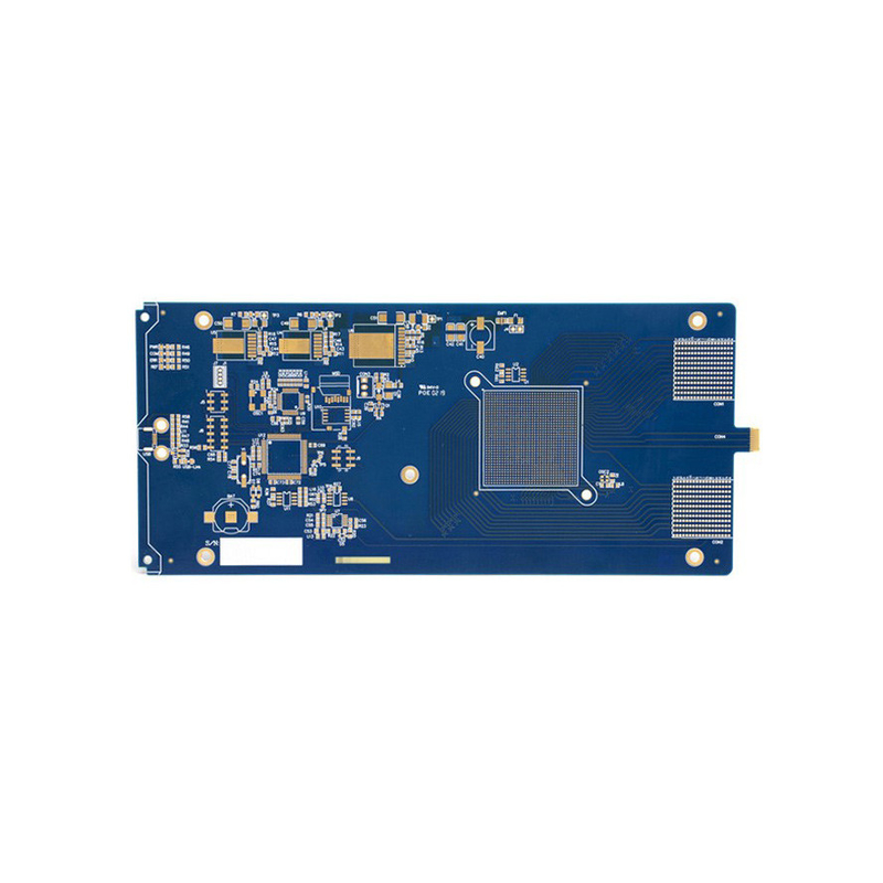
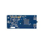
| Product Name: | Altium Designer PCB Prototype Service Double Sided Prototype Circuit Board | Feature: | Altium Designer |
|---|---|---|---|
| Pad(ring): | Min Pad Size For Laser Drillings, Min Pad Size For Mechanical Drillings, Min BGA Pad Size, Pad Size Tolerance | Min. Line Spacing: | 4mil, 0.003", 0.1mm4mil), 0.1mm, 4/4mil(0.1/0.1mm) |
| Min. Line Width: | 4mil, 0.1mm, 0.1mm/4mi, 0.075mm/0.075mm(3mil/3mil), 3mi | Type Of Service: | Turn-Key,Partial Turn-Kye Or Consignment |
| Max Board Size: | 680*550mm Smallest:0.25"*0.25" | Contact Plating: | Au Or Sn Over Ni |
| High Light: | Double Sided Prototype Circuit Board,Altium Designer PCB Prototype Service,ISO14001 PCB Prototype Service |
||
Altium Designer PCB Prototype Service Double Sided Prototype Circuit Board
Lamination in PCB prototype service
INATIONMulti-layer printed circuit boards have trace layers inside the board. This is achieved by laminating a stack of materials in a press by applying pressure and heat for a period of time. This results in an inseparable one piece product. For example, a four-layer PCB can be fabricated by starting from a two-sided copper-clad laminate, etch the circuitry on both sides, then laminate to the top and bottom pre-preg and copper foil. It is then drilled, plated, and etched again to get traces on top and bottom layers.
The inner layers are given a complete machine inspection before lamination because mistakes cannot be corrected afterwards. Automatic optical inspection (AOI) machines compare an image of the board with the digital image generated from the original design data. Automated Optical Shaping (AOS) machines can then add missing copper or remove excess copper using a laser, reducing the number of PCBs that have to be discarded. PCB tracks can have a width of just 10 micrometers.
![]()
Solder resist application in PCB prototype service
Areas that should not be soldered may be covered with solder resist (solder mask). The solder mask is what gives PCBs their characteristic green color, although it is also available in several other colors, such as red, blue, purple, yellow, black and white. One of the most common solder resists used today is called "LPI" (liquid photoimageable solder mask).A photo-sensitive coating is applied to the surface of the PWB in PCB assembly, then exposed to light through the solder mask image film, and finally developed where the unexposed areas are washed away. Dry film solder mask is similar to the dry film used to image the PWB for plating or etching. After being laminated to the PWB surface it is imaged and developed as LPI. Once but no longer commonly used, because of its low accuracy and resolution, is to screen print epoxy ink. In addition to repelling solder, solder resist also provides protection from the environment to the copper that would otherwise be exposed.
PCB Prototype Service Capacities and Technical Specification
| NO. | Items | Capabilities |
| 1 | Layers | 2-68L |
| 2 | Maximum machining size | 600mm*1200mm |
| 3 | Board thickness | 0.2mm-6.5mm |
| 4 | Copper thickness | 0.5oz-28oz |
| 5 | Min trace/space | 2.0mil/2.0mil |
| 6 | Minimum finished aperture | 0. 10mm |
| 7 | Maximum thickness to diameter ratio | 15:1 |
| 8 | Via treatment | Via, blind&buried via, via in pad, Copper in via … |
| 9 | Surface finish/treatment | HASL/HASL lead free, Chemical tin, Chemical Gold, Immersion gold Inmersion Silver/Gold, Osp, Gold Plating |
| 10 | Base Material | FR408 FR408HR, PCL-370HR;IT180A, Megtron 6(Panasonic);Rogers4350, Rogers4003, RO3003, Rogers/Taconic/Arlon/Nelco laminate with FR-4 material(including partial Ro4350B hybrid laminating with FR-4) |
| 11 | Solder mask color | Green.Black.Red.Yellow.White.Blue.Purple.Matte Green. Matte Black |
| 12 | Testing Service | AOI, X-Ray, Flying-Probe, Function Test, First Article Tester |
| 13 | Profiling Punching | Routing,V-CUT,Beveling |
| 14 | Bow&twist | ≤0.5% |
| 15 | HDI type | 1+n+1,2+n+2,3+n+3 |
| 16 | Min mechanical aperture | 0.1mm |
| 17 | Min laser aperture | 0.075mm |
Why choose CESGATE?
CESGATE provides Electronic Manufacturing Services (EMS) for your products that require surface mount, through hole, BGA and mixed technology.
Our main services include PCB prototype service(Electronic assembly), component procurement and PCB fabrication from quick turn, sample run to volume production.
Our customers are who of the Medical, Instrumentation, Intelligent home, Automotive, Consumer electronics industry and Robotics industries.
Full range of PCB manufacturing and assembly services to fit all of your printed circuit board needs.
![]()
![]()
![]()
![]()
![]()
![]()
![]()
FAQ
| Q: Can we inspect quality during production? CESGATE: Yes, we are open and transparent on each production process with nothing to hide. We welcome customer inspect our production process and check in house. |
| Q: What is your inspection policy? How do you control the quality? CESGATE: In order to ensure the quality of PCB products, flying probe inspection is usually used; electrical fixtures, automatic optical inspection (AOI), BGA parts x-ray inspection, first article inspection ( FAI) etc. |
| Q: IS PRODUCT PICTURES AND LABELS AVAILABLE? CESGATE: We will offer after you place an order or before shipment. |
| Q: The lead-free process is required when the circuit board is printed. What should I pay attention to when making the circuit board? CESGATE: The lead-free process during printing is higher than the temperature resistance requirements of the general process, and the temperature resistance requirements must be above 260 °C. Therefore, it is recommended to use a substrate above TG150 when selecting the substrate material. |
| Q: Popular field? CESGATE: Semiconductor, Smart Home, Medical Products, Smart Wearable, Industrial Control, IOT etc. |