
| Place of Origin: | China |
|---|---|
| Brand Name: | CESGATE |
| Certification: | ISO9001/ ISO14001 |
| Model Number: | NA |
| Minimum Order Quantity: | 1PCS( NO MOQ) |
| Price: | Negotiable (Depends on your GERBER and BOM) |
| Packaging Details: | PCB: Vacuum Packing / PCBA: ESD Packing |
| Delivery Time: | 1-30 working days |
| Payment Terms: | T/T, L/C |
| Supply Ability: | 30,000pcs/month |
| Features: | Profiling And V-Scoring | Product Name: | Advanced Flying Probe Testing PCB Prototype Service Profiling And V-Scoring |
|---|---|---|---|
| Buildings: | Rigid-Flex PCB | Pad(ring): | Min Pad Size For Laser Drillings, Min Pad Size For Mechanical Drillings, Min BGA Pad Size, Pad Size Tolerance |
| Min. Line Spacing: | 4mil, 0.003", 0.1mm4mil), 0.1mm, 4/4mil(0.1/0.1mm) | Min. Line Width: | 4mil, 0.1mm, 0.1mm/4mi, 0.075mm/0.075mm(3mil/3mil), 3mi |
| Type: | Rapid Prototyping, Laser Machining, Milling, Broaching, Etching / Chemical Machining | Material: | Aluminum, Copper, Carbon Steel, Stainless Steel, PC |
| High Light: | Flying Probe Testing PCB Prototype,Profiling PCB Prototype Service,V Scoring PCB Prototype Service |
||
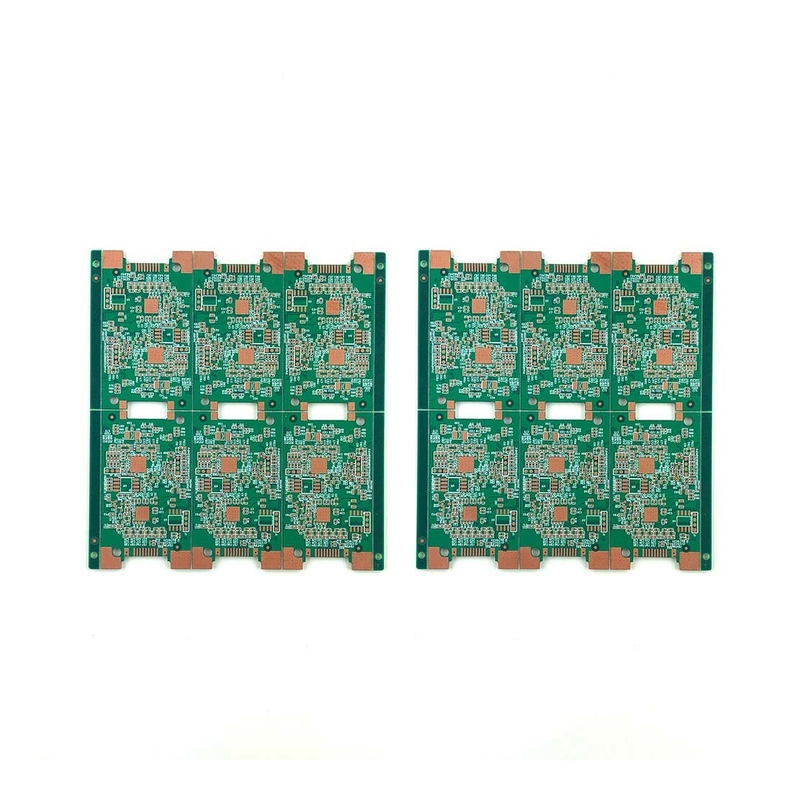
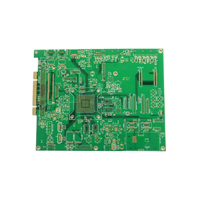
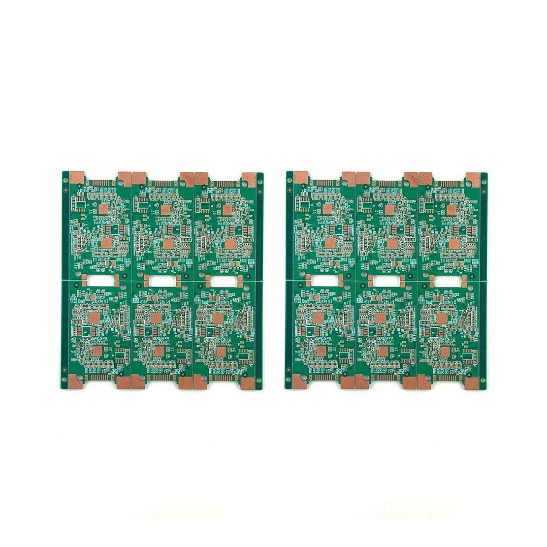
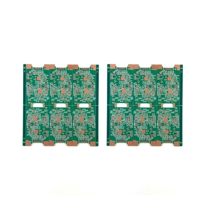
Advanced Flying Probe Testing PCB Prototype Service Profiling And V-Scoring
Types of PCB structures:
The printed circuit board (PCB) structure can be divided into the following three types
Single-Layer PCB: Only one side of the circuit board has copper foil conductors, and the other side has no copper foil conductors at all. The circuits of early electronic products were simple, only one side was needed for connection and conduction, and parts could be placed on the other side without copper foil.
Double-Layer PCB: There are copper foil conductors on both sides of the circuit board, and the paths on the front (Top layer) and the back (Bottom layer) can be connected to each other through vias. Since both sides can be wired, the usable area is twice that of a single panel, which is more suitable for products with complex circuits. The design is to place the part on the front, and the back is the welding surface of the part foot.
Multi-Layer PCB: Multi-Layer PCB is made of multiple etched double-sided boards, an insulating layer (Prepreg) is stacked between the boards, and copper foil is laid on both sides of the outermost layer and then pressed together. Since multiple double-sided laminates are used, the number of layers is usually an even number. The copper foil layer that is pressed inside can be a conduction layer, a signal layer, a power layer or a ground layer. The multi-layer board can theoretically reach more than 50 layers, but the practical application surface is currently up to about 30 layers.
![]()
![]()
The full popularity of printed PCB Prototype circuit boards is due to their convenience in almost all products. Below are several types of PCB Prototype.
Rigid PCB Prototype: These boards are made of fabricated and sturdy materials that are not easily bent or twisted. They are very complex and powerful, with powerful circuits around them. They are easy to handle during repair and maintenance because they are strong and can withstand strong handling. In addition, the components marked on the board are generally clear, and the signal paths are organized.
Flexible Printed Circuit Boards: As the name suggests, these boards are very flexible and are made of the same flexible materials. Flexible PCB Prototype service can be single-sided, double-sided and multi-layered. This design facilitates easy assembly of parts in small or fragile equipment. The flexibility also helps save a lot of space while making the device lighter. These printed PCB Prototype service are best suited for temperature sensitive operating conditions or industrial and related equipment.
Rigid-Flex PCB Prototype service: This is a combination of rigid and flexible PCB Prototype service. These types of PCB Prototype service use multi-layer flex circuits connected to two or more rigid boards. They are lightweight and compact to save space, making them ideal for medical and military applications.
High Frequency PCB Prototype service: This type of board is used for electrical appliances in the frequency range of 500MHz-2GHz. Most frequency sensitive applications, such as microwave and communication systems, use high frequency circuit boards.
Aluminum-Based PCB Prototyp servicee: These have aluminum supports for thermal regulation, high rigidity, and low thermal expansion, and are often used in high-power appliances such as LEDs and power supplies.
Printed PCB Prototype circuit boards have changed and simplified the use of many appliances, from desktop computers to high-end medical equipment, circuit boards are now everywhere
PCB Prototype Service Capacities and Technical Specification
|
Items |
Capabilities |
|
|
1 |
Layers |
2-68L |
|
2 |
Maximum machining size |
600mm*1200mm |
|
3 |
Board thickness |
0.2mm-6.5mm |
|
4 |
Copper thickness |
0.5oz-28oz |
|
5 |
Min trace/space |
2.0mil/2.0mil |
|
6 |
Minimum finished aperture |
0. 10mm |
|
7 |
Maximum thickness to diameter ratio |
15:1 |
|
8 |
Via treatment |
Via, blind&buried via, via in pad, Copper in via … |
|
9 |
Surface finish/treatment |
HASL/HASL lead free, Chemical tin, Chemical Gold, Immersion gold Inmersion Silver/Gold, Osp, Gold Plating |
|
10 |
Base Material |
FR408 FR408HR, PCL-370HR;IT180A, Megtron 6(Panasonic);Rogers4350, |
|
11 |
Solder mask color |
Green.Black.Red.Yellow.White.Blue.Purple.Matte Green. Matte Black |
|
12 |
Testing Service |
AOI, X-Ray, Flying-Probe, Function Test, First Article Tester |
|
13 |
Profiling Punching |
Routing,V-CUT,Beveling |
|
14 |
Bow&twist |
≤0.5% |
|
15 |
HDI type |
1+n+1,2+n+2,3+n+3 |
|
16 |
Min mechanical aperture |
0.1mm |
|
17 |
Min laser aperture |
0.075mm |
Welcome to Chengdu Cesgate Technology Co., Ltd
We can provide one-stop service:
PCB circuit boards+Assembly
E-test.
Electronic components purchasing.
PCB assembly: available on SMT, BGA, DIP.
PCBA function test.
Enclosure assembly.
![]()
![]()
![]()
![]()
![]()
![]()
![]()
FAQ
| Q: Can you give us a preferential discount? CESGATE: Of course, we will offer a preferential discount for your large orders and confirm the order quickly. |
| Q: Why choose us? CESGATE: Professional and experienced R&D team. Advanced production equipment, scientific and reasonable process flow. Reliable and strict quality control system. We test all our products before shipment to make sure everything is in perfect condition. |
| Q: How long does it take for PCB quote? CESGATE: Normally 12 hours to 48 hours as soon as receive internal engineer evaluate confirmation. |
| Q: The Wire Bonding process is required when the circuit board is printed. What should I pay attention to when making the circuit board? CESGATE: When making circuit boards, the surface treatment options are mostly "nickel palladium gold ENEPIG" or "chemical gold ENIG". If the Al aluminum wire is used, the gold thickness is recommended to be 3μ”~5μ”, but if the Au gold wire is used, the gold thickness should preferably be more than 5μ”. |
| Q: The lead-free process is required when the circuit board is printed. What should I pay attention to when making the circuit board? CESGATE: The lead-free process during printing is higher than the temperature resistance requirements of the general process, and the temperature resistance requirements must be above 260 °C. Therefore, it is recommended to use a substrate above TG150 when selecting the substrate material. |
| Q: Can your company provide the serial number when making circuit board text? CESGATE: Serial numbers can be provided, and in addition to text serial numbers, QR-CODE can also be provided for customers to query. |