| Place of Origin: | China |
|---|---|
| Brand Name: | CESGATE |
| Certification: | ISO9001/ ISO14001 |
| Model Number: | NA |
| Minimum Order Quantity: | 1PCS( NO MOQ) |
| Price: | Negotiable (Depends on your GERBER and BOM) |
| Packaging Details: | PCB: Vacuum Packing / PCBA: ESD Packing |
| Delivery Time: | 1-30 working days |
| Payment Terms: | T/T, L/C |
| Supply Ability: | 30,000pcs/month |
| Product Name: | Electronics Prepreg Copper Coin PCB Prototype Service Surface Finish Silkscreen | Buildings: | Prepreg |
|---|---|---|---|
| Pad(ring): | Min Pad Size For Laser Drillings, Min Pad Size For Mechanical Drillings, Min BGA Pad Size, Pad Size Tolerance | Min. Line Spacing: | 4mil, 0.003", 0.1mm4mil), 0.1mm, 4/4mil(0.1/0.1mm) |
| Min. Line Width: | 4mil, 0.1mm, 0.1mm/4mi, 0.075mm/0.075mm(3mil/3mil), 3mi | Min. Hole Size: | 0.2mm, 8 Mil, 0.10mm, 3mil (0.075mm), 0.004" |
| Material Capabilities: | Copper, Aluminum, Stainless Steel, Hardened Metals, Brass | Cnc Machining Or Not: | CNC Machining |
| High Light: | Copper Coin PCB Prototype Service,Prepreg Copper Coin PCB Prototype,Surface Finish Silkscreen Prototype Pcb |
||
Electronics Prepreg Copper Coin PCB Prototype Service Surface Finish Silkscreen
CESGATE's products are widely used in mobile phones, computers, automobiles, communication equipment, servers, industrial control and other electronic information fields. Adhering to the focus on the pressure and challenges of customers in the field of electronic information, to provide customers with competitive circuit boards and services, and continue to create maximum value for customers. Adhere to customer achievement, hard work, open innovation, self-criticism. CESGATE will grow into the world's leading circuit board manufacturer.
![]()
![]()
PCB substrate:
The base material is generally classified according to the insulation, material composition or flame resistance of the substrate. The common raw materials are bakelite, glass fiber, and various plastic boards. Manufacturers of PCB substrates generally use an insulating prepreg composed of glass fiber non-woven fabrics and epoxy resin resins, and then press them with copper foil to form a copper foil substrate for use.
The following are the more common types of PCB substrates:
FR-4: Glass fiber + epoxy resin. It is the most commonly used PCB material, but the Tg is only about 130. If the subsequent processing environment of the product or the operating environment temperature is high, High Tg FR-4 is recommended.
High Tg FR-4: Glass fiber + epoxy resin, the use is second only to FR-4. Tg above 150°C is High Tg.
CEM-1: The center is tissue paper, and the surface is covered with glass cloth + epoxy resin.
CEM-3: The center is glass non-woven cloth, and the surface is covered with glass cloth + epoxy resin.
Ceramic substrate (Ceramic PCB): ceramic powder + glass fiber.
Teflon PCB (Teflon PCB): Teflon + glass fiber.
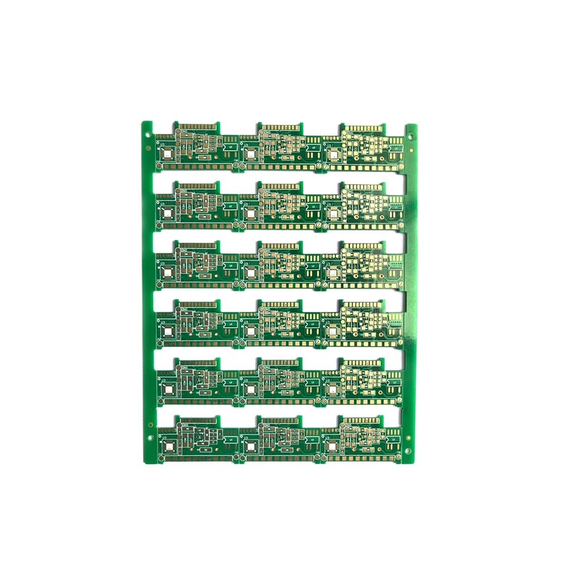
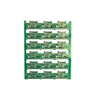
Panel, as the name implies, is to assemble one or several single-board PCB prototype service into the same Panel.
The purpose of the panel:
The original veneer is too small, and it is not easy to pick up after the PCB prototype service is formed or after the PCBA.
After the panels are assembled, the cost of the test fixture and the test man-hours can be saved, and the efficiency can be improved.
The single board is too small or there is no optical point (Fiducial mark) in the single board, but the PCB prototype service has SMT requirements.
There is no hole in the veneer board to fix the PIN for CNC molding, so it is necessary to add a break-away, drill a PIN hole and place an optical point (Fiducial mark).
For the efficiency of SMT printing. At the current speed of the placement machine, the PCB prototype service passes through the placement machine once, and the number of seconds spent on each board will not be too different. Therefore, the utilization of the appropriate single board to form a Panel is relatively high.
Increase the board edge (Break-away) for track conveying during PCBA production.
PCB Prototype Service Capacities and Technical Specification
| NO. | Items | Capabilities |
| 1 | Layers | 2-68L |
| 2 | Maximum machining size | 600mm*1200mm |
| 3 | Board thickness | 0.2mm-6.5mm |
| 4 | Copper thickness | 0.5oz-28oz |
| 5 | Min trace/space | 2.0mil/2.0mil |
| 6 | Minimum finished aperture | 0. 10mm |
| 7 | Maximum thickness to diameter ratio | 15:1 |
| 8 | Via treatment | Via, blind&buried via, via in pad, Copper in via … |
| 9 | Surface finish/treatment | HASL/HASL lead free, Chemical tin, Chemical Gold, Immersion gold Inmersion Silver/Gold, Osp, Gold Plating |
| 10 | Base Material | FR408 FR408HR, PCL-370HR;IT180A, Megtron 6(Panasonic);Rogers4350, Rogers4003, RO3003, Rogers/Taconic/Arlon/Nelco laminate with FR-4 material(including partial Ro4350B hybrid laminating with FR-4) |
| 11 | Solder mask color | Green.Black.Red.Yellow.White.Blue.Purple.Matte Green. Matte Black |
| 12 | Testing Service | AOI, X-Ray, Flying-Probe, Function Test, First Article Tester |
| 13 | Profiling Punching | Routing,V-CUT,Beveling |
| 14 | Bow&twist | ≤0.5% |
| 15 | HDI type | 1+n+1,2+n+2,3+n+3 |
| 16 | Min mechanical aperture | 0.1mm |
| 17 | Min laser aperture | 0.075mm |
![]()
![]()
![]()
![]()
![]()
![]()
![]()
FAQ
| Q: What is your inspection policy? How do you control the quality? CESGATE: In order to ensure the quality of PCB products, flying probe inspection is usually used; electrical fixtures, automatic optical inspection (AOI), BGA parts x-ray inspection, first article inspection ( FAI) etc. |
| Q: What service do you have? CESGATE: We provide turnkey solution including RD, PCB fabrication, SMT, final assembly,testing and other value-added service. |
| Q: What are the main products of your PCB/PCBA services? CESGATE: Our PCB/PCBA services are mainly for the industries including Medical, Automotive, Energy, Metering/Measurements, Consumer Electronics. |
| Q: Is CESGATE a factory or trade company? CESGATE: CESGATE is a factory with PCB factory located in Senzhen and SMT assembly factories in both Shenzhen and Chengdu. |
| Q: Can we inspect quality during production? CESGATE: Yes, we are open and transparent on each production process with nothing to hide. We welcome customer inspect our production process and check in house. |
| Q: How can we ensure our information should not let third party to see our design? CESGATE: We are willing to sign NDA effect by customer side local law and promising to keep customers data in high confidential level. |