| Place of Origin: | China |
|---|---|
| Brand Name: | CESGATE |
| Certification: | UL, IATF16949, ISO9001 |
| Model Number: | NA |
| Minimum Order Quantity: | 1PCS( NO MOQ) |
| Price: | Negotiable (Depends on your GERBER and BOM) |
| Packaging Details: | PCB: Vacuum Packing / PCBA: ESD Packing |
| Delivery Time: | 3-7 working days |
| Payment Terms: | T/T, L/C |
| Supply Ability: | 13kk soldering spot/day |
| Product Name: | Quick Build Small Batch Prototype Assembly Main PCBA 100% Quality Guaranteed | Feature: | 100% Quality Guaranteed |
|---|---|---|---|
| Test: | AOI/SPI/XRAY/First Article Inspection | Design File Format: | Gerber RS-274X BOM (Bill Of Materials) (.xls, .csv, . Xlsx) Centroid (Pick-N-Place/XY File) |
| Types Of Assembly: | THD (Thru-Hole Device), SMT (Surface-Mount Technology), SMT & THD Mixed, 2 Sided SMT And THD Assembly | Component Package: | Reels, Cut Tape, Tube And Tray, Loose Parts And Bulk |
| Necessary Files: | Gerber/BOM/Pick&Place | Maximum Size: | 640 X1100mm |
| High Light: | Prototype Assembly Main PCBA,Small Batch Main PCBA,Quick Build Prototype Pcba |
||
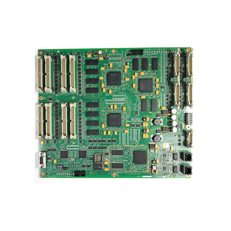
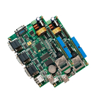
Quick Build Small Batch Prototype Assembly Main PCBA 100% Quality Guaranteed
CESGATE’s Parts Procurement team works concurrently with our PCB Fabrication team to ensure that all assembly materials are received and ready for use as soon as the bare PCBs are ready for assembly. As parts are received at CESGATE’s production facility, our Incoming Quality Control (IQC) team conducts a thorough inspection before warehousing any particular material or component. Inspections include sample operational testing as well as date code verification and entry into a software material management system. Our sophisticated software management system ensures that rules of first-in-first-out are strictly followed, and that parts used in PCB Assembly are always in good working order.
The combined efforts of CESGATE’s IQC and Parts Procurement teams ensure that all parts used in PCB assembly are of the highest quality so that our clients can be confident in the overall shelf-life of their products.
![]()
At Cesgate Electronics, we pride ourselves on our efficient and high-quality turnkey PCB assembly service. Cesgate employs a number of strategies in Quality Management and process control to ensure that every PCB order is done right the first time. In order to achieve the fastest possible turnaround of the highest quality product, we continuously strive to improve our services and to make each step as efficient as possible.
This article provides a step-by-step overview of the standard turnkey PCB assembly process, providing key information at each stage that might relate to a client’s interest. This is a brief overview only, and for those interested in a more detailed elaboration around Cesgate ’s specific capabilities, we recommend reading our comprehensive DFM Guidelines and DFA Guidelines documents.
One of the most important factors in the overall efficiency of each PCB assembly project is the client’s understanding of Cesgate’s process. The number of steps involved in the PCB assembly process depends upon the specific nature of the project in question, as illustrated by the flowchart below, and each of these steps is explained briefly in the following sections. For simplicity’s sake, some intermediary stages are not shown in this flowchart; for example, each stage includes individual inspection upon completion. Being familiar with this process in advance, a savvy engineer can design their PCB specifically for a fast and efficient assembly process by minimizing the overall number of steps required.
![]()
Main PCBA Application - Multilayer Board
Multi-layer board: The required circuits are made on the front and back surfaces of multiple double-sided boards, and an insulating layer (Prepreg) is sandwiched between the two double-sided boards and then pressed together to form several layers of copper. The construction of the wire is usually an even number of layers due to the use of multiple double-sided laminates. The number of copper wires that can be made by multi-layer boards is the largest, and it is used in more complex circuits. At present, the motherboards used in computers mostly use eight-layer boards because of too many components. Generally, small electronic products, such as mobile phones, tablet computers, etc. Due to the requirement of small size, at least an eight-layer board is required. The more electronic components, the smaller the product size, and usually more layers of Main PCBA are required.
1. Material
FR-4 (glass fiber epoxy resin substrate) is the most widely used material in the global electronics industry. FR is a code name for a flame-resistant material grade, which means a material specification that the resin material must be able to self-extinguish after burning. It is not a material name, but a material grade, so there are many types of FR-4 grade materials currently used in general circuit boards, but most of them are four-functional epoxy resin plus filler (Filler) and glass fiber. The composite material made. In recent years, due to the development of electronic product installation technology and Main PCBA technology, FR-4 products with high Tg have appeared again. Tg degree (glass transition temperature - Glass Transition Temperature)
Example: ISOLA FR402, FR408, 370HR South Asia NP-140, NP-155, NP-175
Technical Requirement for main pcba:
Professional Surface-mounting and Through-hole soldering Technology
Various sizes like 1206, 0805, 0603 components SMT technology
ICT(In Circuit Test),FCT(Functional Circuit Test) technology.
Main PCBA With CE, FCC, Rohs Approval
Nitrogen gas reflow soldering technology for SMT.
High Standard SMT&Solder Assembly Line
High density interconnected board placement technology capacity.
Specification
|
Items |
Capabilities |
|
|
1 |
Layers |
2-68L |
|
2 |
Maximum machining size |
600mm*1200mm |
|
3 |
Board thickness |
0.2mm-6.5mm |
|
4 |
Copper thickness |
0.5oz-28oz |
|
5 |
Min trace/space |
2.0mil/2.0mil |
|
6 |
Minimum finished aperture |
0. 10mm |
|
7 |
Maximum thickness to diameter ratio |
15:1 |
|
8 |
Via treatment |
Via, blind&buried via, via in pad, Copper in via … |
|
9 |
Surface finish/treatment |
HASL/HASL lead free, Chemical tin, Chemical Gold, Immersion gold Inmersion Silver/Gold, Osp, Gold Plating |
|
10 |
Base Material |
FR408 FR408HR, PCL-370HR;IT180A, Megtron 6(Panasonic);Rogers4350, |
|
11 |
Solder mask color |
Green.Black.Red.Yellow.White.Blue.Purple.Matte Green. Matte Black |
|
12 |
Testing Service |
AOI, X-Ray, Flying-Probe, Function Test, First Article Tester |
|
13 |
Profiling Punching |
Routing,V-CUT,Beveling |
|
14 |
Bow&twist |
≤0.5% |
|
15 |
HDI type |
1+n+1,2+n+2,3+n+3 |
|
16 |
Min mechanical aperture |
0.1mm |
|
17 |
Min laser aperture |
0.075mm |
![]()
![]()
![]()
![]()
FAQ
| Q: Popular field? CESGATE: Semiconductor, Smart Home, Medical Products, Smart Wearable, Industrial Control, IOT etc. |
| Q: Can you give us a preferential discount? CESGATE: Of course, we will offer a preferential discount for your large orders and confirm the order quickly. |
| Q: Why choose us? CESGATE: Professional and experienced R&D team. Advanced production equipment, scientific and reasonable process flow. Reliable and strict quality control system. We test all our products before shipment to make sure everything is in perfect condition. |
| Q: How long does it take for PCB quote? CESGATE: Normally 12 hours to 48 hours as soon as receive internal engineer evaluate confirmation. |
| Q: The Wire Bonding process is required when the circuit board is printed. What should I pay attention to when making the circuit board? CESGATE: When making circuit boards, the surface treatment options are mostly "nickel palladium gold ENEPIG" or "chemical gold ENIG". If the Al aluminum wire is used, the gold thickness is recommended to be 3μ”~5μ”, but if the Au gold wire is used, the gold thickness should preferably be more than 5μ”. |
| Q: The lead-free process is required when the circuit board is printed. What should I pay attention to when making the circuit board? CESGATE: The lead-free process during printing is higher than the temperature resistance requirements of the general process, and the temperature resistance requirements must be above 260 °C. Therefore, it is recommended to use a substrate above TG150 when selecting the substrate material. |
| Q: Can your company provide the serial number when making circuit board text? CESGATE: Serial numbers can be provided, and in addition to text serial numbers, QR-CODE can also be provided for customers to query. |