| Place of Origin: | China |
|---|---|
| Brand Name: | CESGATE |
| Certification: | UL, IATF16949, ISO9001 |
| Model Number: | NA |
| Minimum Order Quantity: | 1PCS( NO MOQ) |
| Price: | Negotiable (Depends on your GERBER and BOM) |
| Packaging Details: | PCB: Vacuum Packing / PCBA: ESD Packing |
| Delivery Time: | 3-7 working days |
| Payment Terms: | T/T, L/C |
| Supply Ability: | 13kk soldering spot/day |
| Product Name: | Electronic Components Stencil X-Ray Inspection Manufacturer Main PCBA Machine Placement | Feature: | Stencil |
|---|---|---|---|
| Test: | AOI/SPI/XRAY/First Article Inspection | Min Package: | 01005 |
| Order Quantity: | Any Quantities You Need | Design File Format: | Gerber RS-274X BOM (Bill Of Materials) (.xls, .csv, . Xlsx) Centroid (Pick-N-Place/XY File) |
| Types Of Assembly: | THD (Thru-Hole Device), SMT (Surface-Mount Technology), SMT & THD Mixed, 2 Sided SMT And THD Assembly | Component Package: | Reels, Cut Tape, Tube And Tray, Loose Parts And Bulk |
| High Light: | X-Ray Inspection Main PCBA,Main PCBA Machine Placement,UL Electronic PCBA |
||
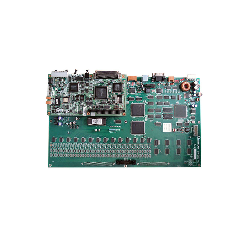
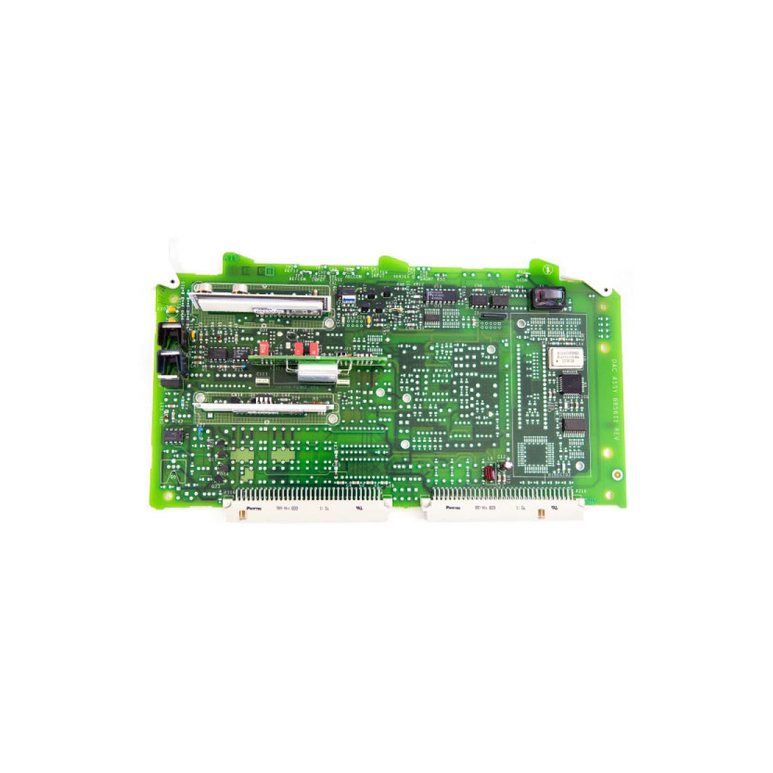
Electronic Components Stencil X-Ray Inspection Manufacturer Main PCBA Machine Placement
At Cesgate Electronics, we pride ourselves on our efficient and high-quality turnkey PCB assembly service. Cesgate employs a number of strategies in Quality Management and process control to ensure that every PCB order is done right the first time. In order to achieve the fastest possible turnaround of the highest quality product, we continuously strive to improve our services and to make each step as efficient as possible.
This article provides a step-by-step overview of the standard turnkey PCB assembly process, providing key information at each stage that might relate to a client’s interest. This is a brief overview only, and for those interested in a more detailed elaboration around Cesgate ’s specific capabilities, we recommend reading our comprehensive DFM Guidelines and DFA Guidelines documents.
One of the most important factors in the overall efficiency of each PCB assembly project is the client’s understanding of Cesgate’s process. The number of steps involved in the PCB assembly process depends upon the specific nature of the project in question, as illustrated by the flowchart below, and each of these steps is explained briefly in the following sections. For simplicity’s sake, some intermediary stages are not shown in this flowchart; for example, each stage includes individual inspection upon completion. Being familiar with this process in advance, a savvy engineer can design their PCB specifically for a fast and efficient assembly process by minimizing the overall number of steps required.
![]()
The first step in the actual PCB Assembly process is the application of solder paste to the bare PCBs. Here the stainless-steel stencil that was created during PCB Fabrication is fit over the bare board, leaving only the pads for assembly of surface-mount components uncovered. The stencil is held in place by a mechanical fixture, and an applicator moves over the surface of the board to meticulously distribute solder paste over those uncovered spaces. Cesgate ’s quality control team then performs a thorough inspection to ensure that the solder has only been applied to the necessary areas, and that all pads are covered with a sufficient amount of paste. For double-sided SMT boards, this process will need to be performed individually for each side, as indicated in the above flowchart.
Cesgate’s solder of choice is SAC305, which is a Lead-Free alloy containing 96.5% tin, 3% silver, and 0.5% copper, and is compliant with the RoHS, REACH, and JEIDA directives. We use the paste version of this material for reflow soldering, and solid versions for manual and wave soldering.
Main PCBA Application - Multilayer Board
Multi-layer board: The required circuits are made on the front and back surfaces of multiple double-sided boards, and an insulating layer (Prepreg) is sandwiched between the two double-sided boards and then pressed together to form several layers of copper. The construction of the wire is usually an even number of layers due to the use of multiple double-sided laminates. The number of copper wires that can be made by multi-layer boards is the largest, and it is used in more complex circuits. At present, the motherboards used in computers mostly use eight-layer boards because of too many components. Generally, small electronic products, such as mobile phones, tablet computers, etc. Due to the requirement of small size, at least an eight-layer board is required. The more electronic components, the smaller the product size, and usually more layers of Main PCBA are required.
1. Material
FR-4 (glass fiber epoxy resin substrate) is the most widely used material in the global electronics industry. FR is a code name for a flame-resistant material grade, which means a material specification that the resin material must be able to self-extinguish after burning. It is not a material name, but a material grade, so there are many types of FR-4 grade materials currently used in general circuit boards, but most of them are four-functional epoxy resin plus filler (Filler) and glass fiber. The composite material made. In recent years, due to the development of electronic product installation technology and Main PCBA technology, FR-4 products with high Tg have appeared again. Tg degree (glass transition temperature - Glass Transition Temperature)
Example: ISOLA FR402, FR408, 370HR South Asia NP-140, NP-155, NP-175
Technical Requirement for main pcba:
Professional Surface-mounting and Through-hole soldering Technology
Various sizes like 1206, 0805, 0603 components SMT technology
ICT(In Circuit Test),FCT(Functional Circuit Test) technology.
Main PCBA With CE, FCC, Rohs Approval
Nitrogen gas reflow soldering technology for SMT.
High Standard SMT&Solder Assembly Line
High density interconnected board placement technology capacity.
Specification
|
Items |
Capabilities |
|
|
1 |
Layers |
2-68L |
|
2 |
Maximum machining size |
600mm*1200mm |
|
3 |
Board thickness |
0.2mm-6.5mm |
|
4 |
Copper thickness |
0.5oz-28oz |
|
5 |
Min trace/space |
2.0mil/2.0mil |
|
6 |
Minimum finished aperture |
0. 10mm |
|
7 |
Maximum thickness to diameter ratio |
15:1 |
|
8 |
Via treatment |
Via, blind&buried via, via in pad, Copper in via … |
|
9 |
Surface finish/treatment |
HASL/HASL lead free, Chemical tin, Chemical Gold, Immersion gold Inmersion Silver/Gold, Osp, Gold Plating |
|
10 |
Base Material |
FR408 FR408HR, PCL-370HR;IT180A, Megtron 6(Panasonic);Rogers4350, |
|
11 |
Solder mask color |
Green.Black.Red.Yellow.White.Blue.Purple.Matte Green. Matte Black |
|
12 |
Testing Service |
AOI, X-Ray, Flying-Probe, Function Test, First Article Tester |
|
13 |
Profiling Punching |
Routing,V-CUT,Beveling |
|
14 |
Bow&twist |
≤0.5% |
|
15 |
HDI type |
1+n+1,2+n+2,3+n+3 |
|
16 |
Min mechanical aperture |
0.1mm |
|
17 |
Min laser aperture |
0.075mm |
![]()
![]()
![]()
![]()
FAQ
| Q: Are my files safe? CEGSATE: Your files are kept very safe, and we are protecting intellectual property for our clients throughout the process. All files provided by customers are never shared with any third party. |
| Q: MOQ? CESGATE: There is no MOQ in POE. We are able to flexibly handle small and large batches. |
| Q: Do you have any other services? CESGATE: We mainly focus on the procurement services of PCB + assembly + components. In addition, we can also provide programming, testing, cable, housing assembly services. |
| Q: What is your inspection policy? How do you control the quality? CESGATE: In order to ensure the quality of PCB products, flying probe inspection is usually used; electrical fixtures, automatic optical inspection (AOI), BGA parts x-ray inspection, first article inspection ( FAI) etc. |
| Q: What service do you have? CESGATE: We provide turnkey solution including RD, PCB fabrication, SMT, final assembly,testing and other value-added service. |
| Q: What are the main products of your PCB/PCBA services? CESGATE: Our PCB/PCBA services are mainly for the industries including Medical, Automotive, Energy, Metering/Measurements, Consumer Electronics. |
| Q: Is CESGATE a factory or trade company? CESGATE: CESGATE is a factory with PCB factory located in Senzhen and SMT assembly factories in both Shenzhen and Chengdu. |