| Place of Origin: | China |
|---|---|
| Brand Name: | CESGATE |
| Certification: | UL, IATF16949, ISO9001 |
| Model Number: | NA |
| Minimum Order Quantity: | 1PCS( NO MOQ) |
| Price: | Negotiable (Depends on your GERBER and BOM) |
| Packaging Details: | PCB: Vacuum Packing / PCBA: ESD Packing |
| Delivery Time: | 3-7 working days |
| Payment Terms: | T/T, L/C |
| Supply Ability: | 13kk soldering spot/day |
| Product Name: | Pin Through Hole Wave Soldering PCB Assembly Service Blind Via Printing | Feature: | Blind Via |
|---|---|---|---|
| Minimum Line Width: | 3 Mil | Minimum Spacing: | 4 Mil |
| Minimum Aperture: | 0.2mm | Maximum Board Thickness: | 6mm |
| Maximum Size: | 640 X1100mm | Min. Line Width: | 3mi,0.2mm,0.15mm,0.1 0mm,0.075mm/0.075mm(3mil/3mil) |
| High Light: | Wave Soldering PCB Assembly Service,Soldering PCB Assembly Service,Blind Via Printing PCB Assembly |
||
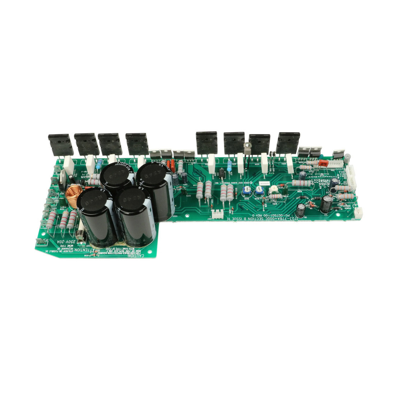
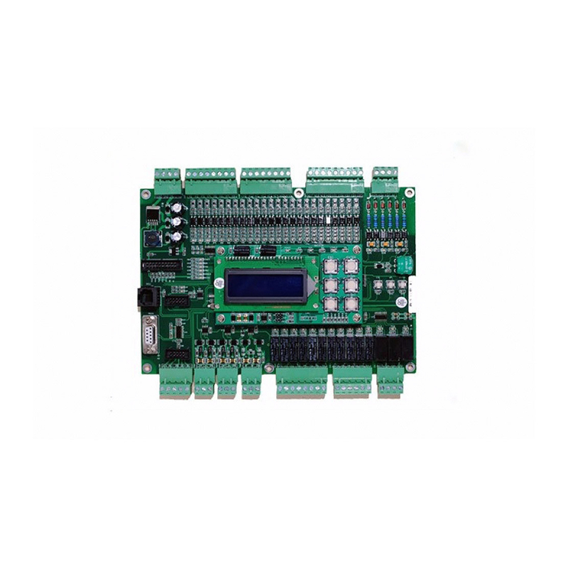
Pin Through Hole Wave Soldering PCB Assembly Service Blind Via Printing
Features of PCB ASSEMBLY:
PCB assembly is the abbreviation of Printed Circuit Board Assembly, which means that PCB assembly is loaded by SMT from the PCB empty board, and then goes through the whole process of DIP plug-in. Note: Both SMT and DIP are ways of integrating parts on a PCB. The main difference is that SMT does not require drilling holes in the PCB. In DIP, the PIN pins of the part need to be inserted into the already drilled holes. SMT (Surface Mounted Technology) surface mount technology mainly uses a placement machine to mount some tiny parts on a PCB. The production process is: PCB board positioning, solder paste printing, placement machine installation, reflow oven and finished product inspection. DIP means "plug-in", that is, inserting parts on the PCB board. This is to integrate parts in the form of plug-ins when some parts are larger in size and not suitable for placement technology. The main production processes are: glue, plug-in, inspection, wave soldering, printing, finished product inspection.
![]()
![]()
Technical Requirement for PCB Assembly
Quality Control of CESGATE PCB Assembly
Specification
|
Items |
Capabilities |
|
|
1 |
Layers |
2-68L |
|
2 |
Maximum machining size |
600mm*1200mm |
|
3 |
Board thickness |
0.2mm-6.5mm |
|
4 |
Copper thickness |
0.5oz-28oz |
|
5 |
Min trace/space |
2.0mil/2.0mil |
|
6 |
Minimum finished aperture |
0. 10mm |
|
7 |
Maximum thickness to diameter ratio |
15:1 |
|
8 |
Via treatment |
Via, blind&buried via, via in pad, Copper in via … |
|
9 |
Surface finish/treatment |
HASL/HASL lead free, Chemical tin, Chemical Gold, Immersion gold Inmersion Silver/Gold, Osp, Gold Plating |
|
10 |
Base Material |
FR408 FR408HR, PCL-370HR;IT180A, Megtron 6(Panasonic);Rogers4350, |
|
11 |
Solder mask color |
Green.Black.Red.Yellow.White.Blue.Purple.Matte Green. Matte Black |
|
12 |
Testing Service |
AOI, X-Ray, Flying-Probe, Function Test, First Article Tester |
|
13 |
Profiling Punching |
Routing,V-CUT,Beveling |
|
14 |
Bow&twist |
≤0.5% |
|
15 |
HDI type |
1+n+1,2+n+2,3+n+3 |
|
16 |
Min mechanical aperture |
0.1mm |
|
17 |
Min laser aperture |
0.075mm |
Company Profile
CESGATE with customers to provide them with the highest-quality PCB and PCB assembly electronic manufacturing services to achieve their goals. Our flexibility is in meeting customer requirements and our superior customer service. We help companies introduce their new products to market in the fastest time possible by providing high quality, quick-turn assembly.We provide one-stop electronic manufacturing service to help you qualify your designs and provide quality samples to your customers.
![]()
![]()
![]()
![]()
FAQ
| Q: WHAT IS YOUR TERMS OF PACKING? CESGATE: Generally, we pack our goods in neutral white boxes and brown cartons. |
| Q: WHAT IS YOUR MOQ? CESGATE: MOQ is SPQ normally, while it depends on your specific order. (Sample is available if the buyer can afford the shipping fee.) |
| Q: DO YOU TEST ALL YOUR GOODS BEFORE DELIVERY? CESGATE: 1. Our products are all original, and we will test the goods before shipment by professional machines like KEYSIGHT E4991A and KEYSIGHT E4980. 2. If The buyer need Test Report, we can send the product to anthoritative institution such as White horse Laboratories(SZ) Limited,Global Electronics Testing,etc. |
| Q: HOW DO YOU MAKE OUR BUSINESS LONG-TERM AND GOOD RELATIONSHIP? CESGATE: 1. We would like to offer sample if the buyer really want to make long-term relationship with us. 2. We keep good quality and competitive price to ensure our customers benefit. 3. We respect customers as our friend and sincerely do business and make friends with them,no matter where they come from. |
| Q: Do you support fast proofing? CESGATE: Yes, we support fast proofing within 3-7 days. |