| Place of Origin: | China |
|---|---|
| Brand Name: | CESGATE |
| Certification: | ISO9001/ ISO14001 |
| Model Number: | NA |
| Minimum Order Quantity: | 1PCS( NO MOQ) |
| Price: | Negotiable (Depends on your GERBER and BOM) |
| Packaging Details: | PCB: Vacuum Packing / PCBA: ESD Packing |
| Delivery Time: | 1-30 working days |
| Payment Terms: | T/T, L/C |
| Supply Ability: | 30,000pcs/month |
| Features: | Rapid Prototyping Processing | Product Name: | Rapid Production Processing Electronics Samples PCB Prototype Service |
|---|---|---|---|
| Pad(ring): | Min Pad Size For Laser Drillings, Min Pad Size For Mechanical Drillings, Min BGA Pad Size, Pad Size Tolerance | Min. Line Spacing: | 4mil, 0.003", 0.1mm4mil), 0.1mm, 4/4mil(0.1/0.1mm) |
| Min. Line Width: | 4mil, 0.1mm, 0.1mm/4mi, 0.075mm/0.075mm(3mil/3mil), 3mi | Type: | Rapid Prototyping, Laser Machining, Milling, Broaching, Etching / Chemical Machining |
| Keyword: | CNC Macining Parts, Aluminum Profile, Prototyping Supplier Rapid Prototyping 2D&3D Drawing Design, Led Pcb Connector, Plastic Prototype Fabrication | Packing: | Poly Bag + Inner Box + Carton, Packed In Plastic Bag With Carton For Outer Packing Or As Your Request, Polybag, Inner-Plastic Bag; Outer -Standard Carton Box. |
| High Light: | 4mil Rapid Prototyping Processing Circuit Card,0.1mm PCB Prototype Service |
||
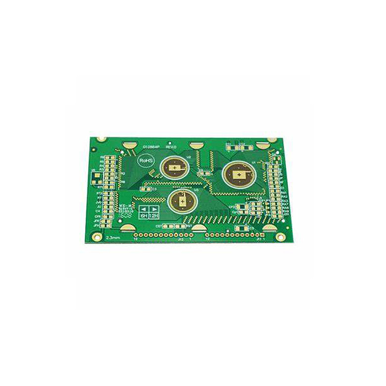
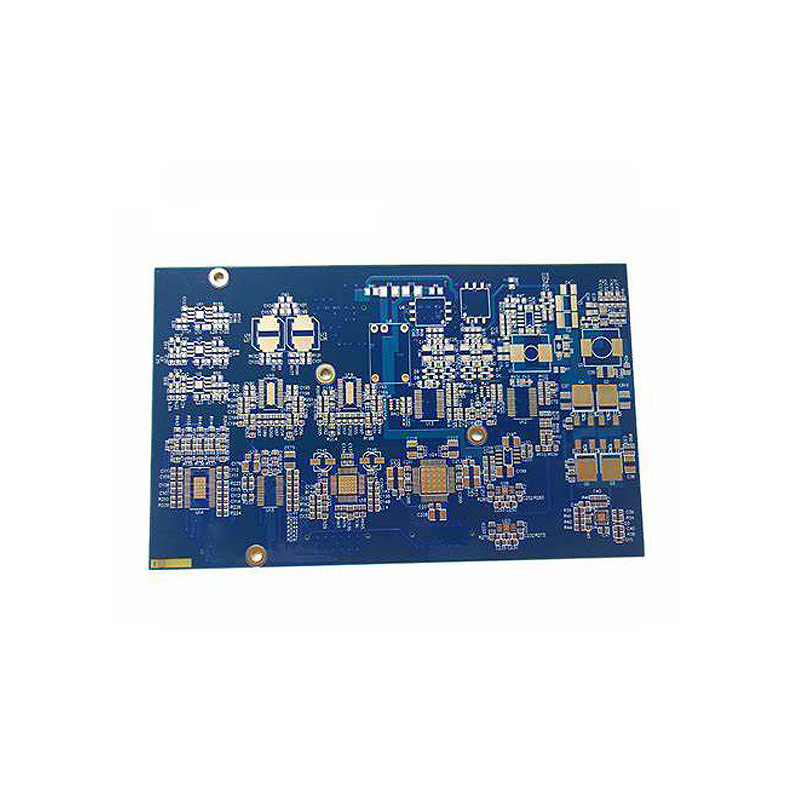
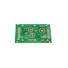
Rapid Production Processing Electronics Samples PCB Prototype Service
PCB Prototype inspection method:
PCB Prototype inspection methods include appearance optical inspection and electrical path test
AOI (Auto Optical Inspection):
It is the automatic optical recognition system. Based on the consideration of production efficiency and inspection accuracy, the use of optical identification instruments to replace manual visual inspection (Visual Inspection) is already a very basic process. The principle of AOI is to first save the standard image file in the device, use the image file to perform optical comparison with the measured object, and automatically determine whether the error of the measured object exceeds the standard. Scrap or repair. Since the circuits on the circuit boards are getting more and more fine, it has already exceeded the limit that can be found by the human eye. Therefore, the AOI equipment of the PCB Prototype is mostly used to check and compare the circuit layers, and compare whether there is too much or too little etching or damage such as collisions.
![]()
![]()
Why choose CESGATE?
QUALITY
All PCB Prototype service are 100% electrical tested. They can pick and send PCBs to E-fixture test machines automatically, and place the PCB Prototype at appointed places after testing, according to the test result;All PCBs are 100% visually inspected. All tests and inspect results are recorded in the inspection report and shipped together with the PCB Prototype.
EXEPERIENCE
More than 10 years of experiences in the production of PCB Prototype service .
Professional Engineer and oversea sales team in the PCB Prototype service industry fully involved in the whole business procedures.Designed and manufactured various complex PCB Prototype, which can meet all your design and manufacturing needs.
Equipment
More than 80% are automated production equipment, improves the production efficiency and product quality.And a variety of famous brand equipment is used in all processes, including Drilling, Electroless Plating, Electroplating, Etching, Solder Mask, Silk Screen, Chemical Gold, Electrolytic Gold, CNC Profiling,Electrical Testing, and Packing.
Price
Since we are directly operated by the factory, intermediate links are omitted. Secondly, we have a complete supply chain management system to control the cost of production, manufacturing and procurement sources. We will give you the cheapest purchase price to compare with other factories or manufacturers while ensuring good quality.
PCB Prototype Service Capacities and Technical Specification
|
Items |
Capabilities |
|
|
1 |
Layers |
2-68L |
|
2 |
Maximum machining size |
600mm*1200mm |
|
3 |
Board thickness |
0.2mm-6.5mm |
|
4 |
Copper thickness |
0.5oz-28oz |
|
5 |
Min trace/space |
2.0mil/2.0mil |
|
6 |
Minimum finished aperture |
0. 10mm |
|
7 |
Maximum thickness to diameter ratio |
15:1 |
|
8 |
Via treatment |
Via, blind&buried via, via in pad, Copper in via … |
|
9 |
Surface finish/treatment |
HASL/HASL lead free, Chemical tin, Chemical Gold, Immersion gold Inmersion Silver/Gold, Osp, Gold Plating |
|
10 |
Base Material |
FR408 FR408HR, PCL-370HR;IT180A, Megtron 6(Panasonic);Rogers4350, |
|
11 |
Solder mask color |
Green.Black.Red.Yellow.White.Blue.Purple.Matte Green. Matte Black |
|
12 |
Testing Service |
AOI, X-Ray, Flying-Probe, Function Test, First Article Tester |
|
13 |
Profiling Punching |
Routing,V-CUT,Beveling |
|
14 |
Bow&twist |
≤0.5% |
|
15 |
HDI type |
1+n+1,2+n+2,3+n+3 |
|
16 |
Min mechanical aperture |
0.1mm |
|
17 |
Min laser aperture |
0.075mm |
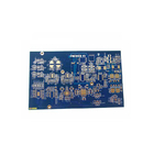
Application advantages of multilayer circuit boards:
1. High assembly density, small size and light weight, meeting the needs of lightweight and miniaturization of electronic equipment;
2. Due to the high assembly density, the wiring between components (including components) is reduced, the installation is simple, and the reliability is high;
3. Due to the repeatability and consistency of the graphics, wiring and assembly errors are reduced, and equipment maintenance, debugging and inspection time are saved;
4. The number of wiring layers can be increased, thereby increasing design flexibility;
5. It can form a circuit with a certain impedance, and can form a high-speed transmission circuit;
6. The circuit and magnetic circuit shielding layer can be set, and the metal core heat dissipation layer can also be set to meet the needs of special functions such as shielding and heat dissipation.
![]()
![]()
![]()
![]()
![]()
![]()
![]()
FAQ
|
Q: The lead-free process is required when the circuit board is printed. What should I pay attention to when making the circuit board? |
|
Q: Can your company provide the serial number when making circuit board text? |
|
Q: How long is the shelf life of the PCB Prototype board and how should it be stored? |
|
Q: What is your delivery date? |