| Place of Origin: | China |
|---|---|
| Brand Name: | CESGATE |
| Certification: | ISO9001/ ISO14001 |
| Model Number: | NA |
| Minimum Order Quantity: | 1PCS( NO MOQ) |
| Price: | Negotiable (Depends on your GERBER and BOM) |
| Packaging Details: | PCB: Vacuum Packing / PCBA: ESD Packing |
| Delivery Time: | 1-30 working days |
| Payment Terms: | T/T, L/C |
| Supply Ability: | 30,000pcs/month |
| Product Name: | Rogers 4350 Prototype Smt Assembly PCB Prototype Service Alternative Bom Sap | Material: | Aluminum, Brass, Bronze, Copper, Hardened Metals, Stainless Steel, Steel |
|---|---|---|---|
| Optional Service: | 3 4 5 6 Axis CNC Machining Service | Min. Line Spacing: | 4mil, 0.003", 0.1mm4mil), 0.1mm, 4/4mil(0.1/0.1mm) |
| Min. Line Width: | 4mil, 0.1mm, 0.1mm/4mi, 0.075mm/0.075mm(3mil/3mil), 3mi | Min. Hole Size: | 0.2mm, 8 Mil, 0.10mm, 3mil (0.075mm), 0.004" |
| Drawing Format: | 2D(PDF/CAD) And 3D(IGES/STEP) | OEM/ODM: | OEM ODM CNC Machining Services |
| High Light: | Rogers 4350 PCB Prototype Service,Rogers 4350 high frequency pcb design,high frequency pcb design OEM ODM |
||
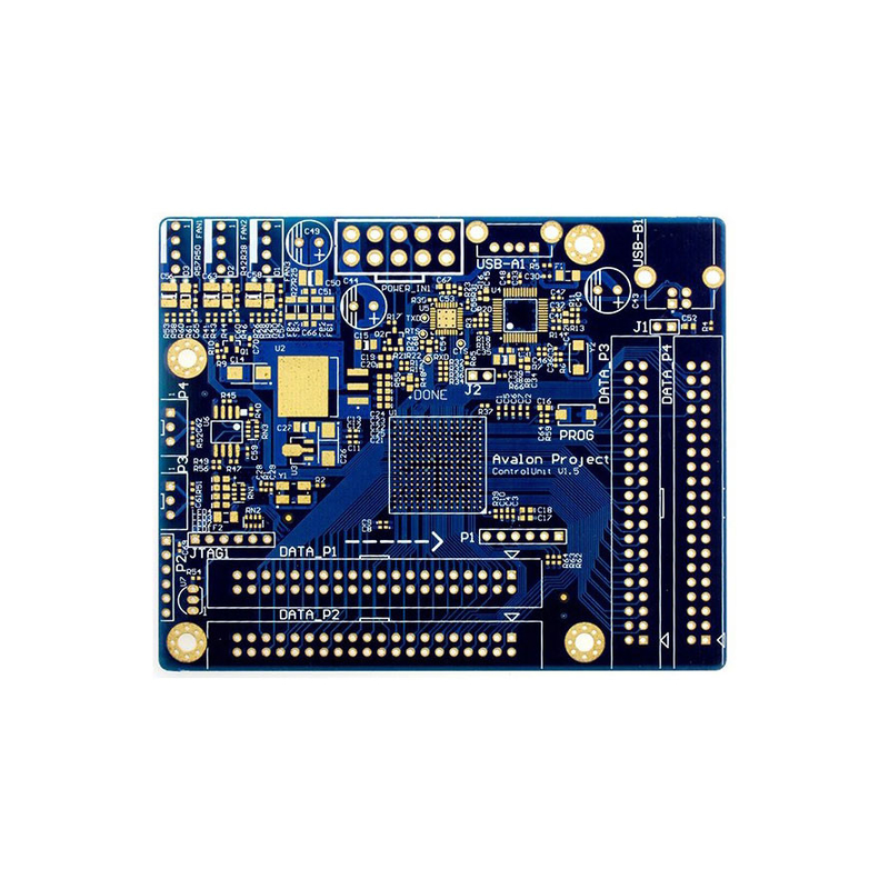
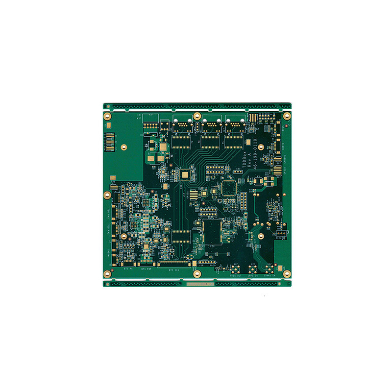
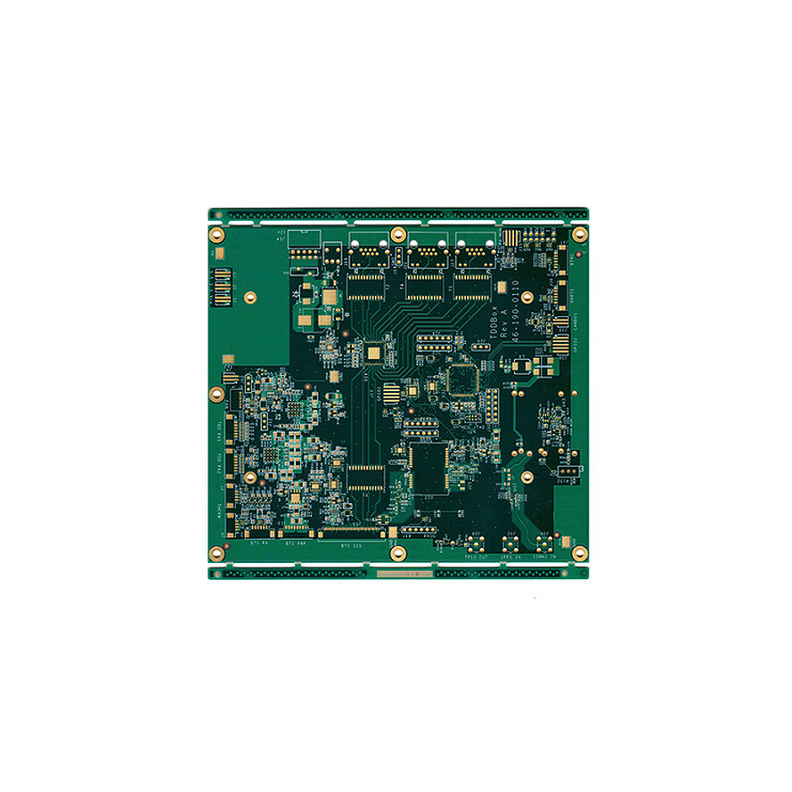
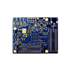
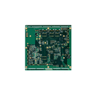
Rogers 4350 Prototype Smt Assembly PCB Prototype Service Alternative Bom Sap
Briefly introduce our PCBs
PCB Process - Introduction to HDI
HDI (High Density Interconnect): High-density interconnection technology, mainly using micro-blind / buried vias (blind / buried vias), a technology that makes PCB circuit board circuit distribution density higher. The advantage is that it can greatly increase the usable area of the PCB circuit board, making the product as miniaturized as possible. However, due to the increase in line distribution density, it is impossible to use traditional drilling methods to drill through holes, and some of the via holes must be drilled with laser drilling to form blind holes, or cooperate with inner-layer buried vias to interconnect.Generally, the diameter of the laser drilling hole is designed to be 3 ~ 4 mil (about 0.076 ~ 0.1 mm), and the insulation thickness between each laser drilling layer is about 3 mil. Due to the use of laser drilling many times, the key to the quality of the HDI circuit board is the hole pattern after laser drilling and whether the hole can be evenly filled after the subsequent electroplating and filling.
The following are examples of HDI board types. The pink holes in the picture are blind holes, which are made by laser drilling, and the diameter is usually 3 to 4 mil; the yellow holes are buried holes, which are made by mechanical drilling, and the diameter is at least 6 mil (0.15 mm).
PCB prototype service Capacities and Technical Specification
| NO. | Items | Capabilities |
| 1 | Layers | 2-68L |
| 2 | Maximum machining size | 600mm*1200mm |
| 3 | Board thickness | 0.2mm-6.5mm |
| 4 | Copper thickness | 0.5oz-28oz |
| 5 | Min trace/space | 2.0mil/2.0mil |
| 6 | Minimum finished aperture | 0. 10mm |
| 7 | Maximum thickness to diameter ratio | 15:1 |
| 8 | Via treatment | Via, blind&buried via, via in pad, Copper in via … |
| 9 | Surface finish/treatment | HASL/HASL lead free, Chemical tin, Chemical Gold, Immersion gold Inmersion Silver/Gold, Osp, Gold Plating |
| 10 | Base Material | FR408 FR408HR, PCL-370HR;IT180A, Megtron 6(Panasonic);Rogers4350, Rogers4003, RO3003, Rogers/Taconic/Arlon/Nelco laminate with FR-4 material(including partial Ro4350B hybrid laminating with FR-4) |
| 11 | Solder mask color | Green.Black.Red.Yellow.White.Blue.Purple.Matte Green. Matte Black |
| 12 | Testing Service | AOI, X-Ray, Flying-Probe, Function Test, First Article Tester |
| 13 | Profiling Punching | Routing,V-CUT,Beveling |
| 14 | Bow&twist | ≤0.5% |
| 15 | HDI type | 1+n+1,2+n+2,3+n+3 |
| 16 | Min mechanical aperture | 0.1mm |
| 17 | Min laser aperture | 0.075mm |
PCBA Capabilities
Briefly Introduce Our Strength
1. The production of circuit board equipment is very important. Before looking for a supplier, most users will know about a manufacturer with a good reputation in the industry. The production equipment of a good PCB circuit board factory will never get worse, and customers can judge the production strength of the circuit board manufacturer by analyzing the production equipment and scale of the circuit board manufacturer.
2. When making PCB double-sided, every process is important. Any prototype PCB service circuit board manufacturer will have professional inspectors. Only 100% qualified products will be shipped to customers. For PCB manufacturers with very high product requirements that pass strict inspection procedures, the one-time pass rate can reach more than 98%.
3. Before ordering circuit board prototype PCB service production, you should know the qualification certificate of the PCB circuit board manufacturer. Don't underestimate these certificates. We can use it to know the establishment date of the manufacturer. A qualified PCB factory can survive. There must be some truth to it.
Application
There are many types of multilayer circuit boards with different names. Can be named according to material, number of layers, inherent characteristics, etc., such as: single-sided, double-sided, multi-layer, HDI, Allegro, FR4 circuit board, ceramic circuit PCB, alumina ceramic circuit board, aluminum nitride ceramic circuit board, circuit board , prototype PCB service board, aluminum substrate, high frequency board, thick copper board, impedance board, PCB, ultra-thin circuit board, ultra-thin circuit board, printed (copper etching technology) circuit board, etc. The circuit board is a miniaturized and intuitive circuit, which plays an important role in the mass production of fixed circuits and the optimization of electrical layout.Since printed circuit boards are used in electronic equipment, manual wiring errors are avoided and automatic insertion, soldering and inspection are realized. This can ensure the quality and reliability of electronic products, improve labor productivity, reduce production costs, and facilitate maintenance.
![]()
![]()
![]()
![]()
![]()
![]()
![]()
FAQ
|
Q: Which express companies do you cooperate with? |
| Q: What is the difference between the HDI board and the general circuit board? CESGATE: Most of HDI use laser to form holes, while general circuit boards only use mechanical drilling, and HDI boards are manufactured by the build-up method (Build Up), so more layers will be added, while general circuit boards are only added once. |
| Q: How long does it take for PCB quote? CESGATE: Normally 12 hours to 48 hours as soon as receive internal engineer evaluate confirmation. |
| Q: Can your company provide the serial number when making circuit board text? CESGATE: Serial numbers can be provided, and in addition to text serial numbers, QR-CODE can also be provided for customers to query. |
| Q: Why choose us? CESGATE: Professional and experienced R&D team. Advanced production equipment, scientific and reasonable process flow. Reliable and strict quality control system. We test all our products before shipment to make sure everything is in perfect condition. |
| Q: What modes of transport are there? CESGATE: Usually includes express, air shipment, rail shipment and sea shipment. |