| Place of Origin: | China |
|---|---|
| Brand Name: | CESGATE |
| Certification: | ISO9001/ ISO14001 |
| Model Number: | NA |
| Minimum Order Quantity: | 1PCS( NO MOQ) |
| Price: | Negotiable (Depends on your GERBER and BOM) |
| Packaging Details: | PCB: Vacuum Packing / PCBA: ESD Packing |
| Delivery Time: | 1-30 working days |
| Payment Terms: | T/T, L/C |
| Supply Ability: | 30,000pcs/month |
| Product Name: | 12v Audio Amplifier Circuit Board Board PCB Prototype Service Cs01 In Sap | Application: | Auto Spare Parts,machine Parts,Electronic Accessories |
|---|---|---|---|
| Optional Service: | 3 4 5 6 Axis CNC Machining Service | Min. Line Spacing: | 4mil, 0.003", 0.1mm4mil), 0.1mm, 4/4mil(0.1/0.1mm) |
| Min. Line Width: | 4mil, 0.1mm, 0.1mm/4mi, 0.075mm/0.075mm(3mil/3mil), 3mi | Min. Hole Size: | 0.2mm, 8 Mil, 0.10mm, 3mil (0.075mm), 0.004" |
| Drawing Format: | 2D(PDF/CAD) And 3D(IGES/STEP) | Process: | CNC Macining, Turning, Milling, EDM |
| High Light: | EDM audio amplifier circuit board,CNC Machining 12v audio amplifier board,6 Axis 12v audio amplifier board |
||
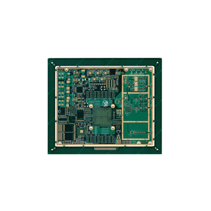
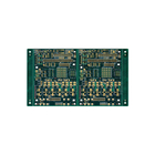
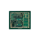
12v Audio Amplifier Circuit Board Board PCB Prototype Service Cs01 In Sap
Briefly introduce our PCBs
PCB inspection methods include appearance optical inspection and electrical path test
AOI (Auto Optical Inspection):
It is the automatic optical recognition system. Based on the consideration of production efficiency and inspection accuracy, the use of optical identification instruments to replace manual visual inspection (Visual Inspection) is already a very basic process. The principle of AOI is to first save the standard image file in the device, use the image file to perform optical comparison with the measured object, and automatically determine whether the error of the measured object exceeds the standard. Scrap or repair. Since the circuits on the circuit boards are getting more and more fine, it has already exceeded the limit that can be found by the human eye. Therefore, the AOI equipment of the PCB prototype service is mostly used to check and compare the circuit layers, and compare whether there is too much or too little etching or damage such as collisions. .
PCB prototype service Capacities and Technical Specification
| NO. | Items | Capabilities |
| 1 | Layers | 2-68L |
| 2 | Maximum machining size | 600mm*1200mm |
| 3 | Board thickness | 0.2mm-6.5mm |
| 4 | Copper thickness | 0.5oz-28oz |
| 5 | Min trace/space | 2.0mil/2.0mil |
| 6 | Minimum finished aperture | 0. 10mm |
| 7 | Maximum thickness to diameter ratio | 15:1 |
| 8 | Via treatment | Via, blind&buried via, via in pad, Copper in via … |
| 9 | Surface finish/treatment | HASL/HASL lead free, Chemical tin, Chemical Gold, Immersion gold Inmersion Silver/Gold, Osp, Gold Plating |
| 10 | Base Material | FR408 FR408HR, PCL-370HR;IT180A, Megtron 6(Panasonic);Rogers4350, Rogers4003, RO3003, Rogers/Taconic/Arlon/Nelco laminate with FR-4 material(including partial Ro4350B hybrid laminating with FR-4) |
| 11 | Solder mask color | Green.Black.Red.Yellow.White.Blue.Purple.Matte Green. Matte Black |
| 12 | Testing Service | AOI, X-Ray, Flying-Probe, Function Test, First Article Tester |
| 13 | Profiling Punching | Routing,V-CUT,Beveling |
| 14 | Bow&twist | ≤0.5% |
| 15 | HDI type | 1+n+1,2+n+2,3+n+3 |
| 16 | Min mechanical aperture | 0.1mm |
| 17 | Min laser aperture | 0.075mm |
PCBA Capabilities
Briefly Introduce Our Strength
1. Provide full BOM component supply and part selection
2. From the original factory and the first-level agents, the original authentic guarantee
3. More than 50,000 kinds of components are always in stock
4. Customers can buy on demand, no need to buy the whole package
Application
Printed circuit boards are mainly composed of insulating substrates and conductors, which play the role of support, interconnection and part of circuit elements in electronic equipment. Electronic components such as integrated circuits, resistors, capacitors, etc. cannot function as a single entity. They only work as a whole if they have a firm foothold on the PCB prototype service and there are conductive junctions connecting them. PCB prototype service is the skeleton that supports the components and is the conduit for connecting electrical signals. In addition, some printed circuit boards have components such as resistors, capacitors, inductors, etc., which become functional circuits and play the role of trachea.The role of printed circuit boards in electronic equipment is to provide mechanical support for fixing and assembling for transistors, integrated circuits, resistors, capacitors, inductors and other components; to realize the integration of transistors, integrated circuits, resistors, capacitors, inductors and other components. Wiring and electrical connection and electrical insulation between components meet their electrical characteristics; provide identification characters and graphics for the inspection and maintenance of components in the electronic assembly process, and provide solder resist graphics for wave soldering.Since printed circuit boards are used in electronic equipment, manual wiring errors are avoided and automatic insertion, soldering and inspection are realized. This can ensure the quality and reliability of electronic products, improve labor productivity, reduce production costs, and facilitate maintenance.
![]()
![]()
![]()
![]()
![]()
![]()
![]()
FAQ
|
Q: What are the common substrates of CESGATE? |
| Q: What is the difference between the HDI board and the general circuit board? CESGATE: Most of HDI use laser to form holes, while general circuit boards only use mechanical drilling, and HDI boards are manufactured by the build-up method (Build Up), so more layers will be added, while general circuit boards are only added once. |
| Q: What does CESGATE need for a customized PCBA order? CESGATE: When you place a PCBA order, you need to provide Gerber or pcb file and the BOM list to us. |
| Q: What certificates do you have? CESGATE: We have ISO 9001, ISO14001 and UL certificates.Q: Can you give us a preferential discount? CESGATE: Of course, we will offer a preferential discount for your large orders and confirm the order quickly. |
| Q: Can your company provide the serial number when making circuit board text? CESGATE: Serial numbers can be provided, and in addition to text serial numbers, QR-CODE can also be provided for customers to query. |
| Q: What modes of transport are there? CESGATE: Usually includes express, air shipment, rail shipment and sea shipment. |