| Place of Origin: | China |
|---|---|
| Brand Name: | CESGATE |
| Certification: | ISO9001/ ISO14001 |
| Model Number: | NA |
| Minimum Order Quantity: | 1PCS( NO MOQ) |
| Price: | Negotiable (Depends on your GERBER and BOM) |
| Packaging Details: | PCB: Vacuum Packing / PCBA: ESD Packing |
| Delivery Time: | 1-30 working days |
| Payment Terms: | T/T, L/C |
| Supply Ability: | 30,000pcs/month |
| Product Name: | Cadence Allegro Assembly Languages PCB Prototype Service Bom Management | Copper Thickness: | 1oz, 1/2OZ 1OZ 2OZ 3OZ, 2oz, 1oz(35um), 0.5-3.0 Oz |
|---|---|---|---|
| Base Material: | FR-4, Etc, Alu, High TG, FR-4/ceramic/cem-3/FR-1 | Min. Line Spacing: | 4mil, 0.003", 0.1mm4mil), 0.1mm, 4/4mil(0.1/0.1mm) |
| Min. Line Width: | 4mil, 0.1mm, 0.1mm/4mi, 0.075mm/0.075mm(3mil/3mil), 3mi | Certificate: | ISO9001, ISO16949, ROHS |
| Surface Finishing: | HASL, OSP, HASL Lead Free, ENIG, Immersion Gold | Testing Service: | AOI X-Ray, 100% Function Test, |
| High Light: | 1oz Copper pcb printing service,1oz Copper Fabrication PCB Prototype,Fabrication PCB Prototype ISO16949 |
||
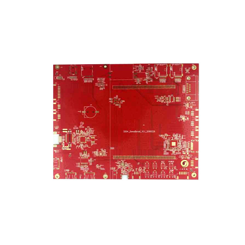
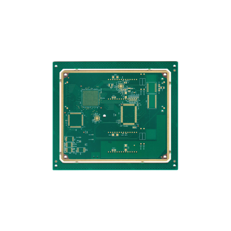
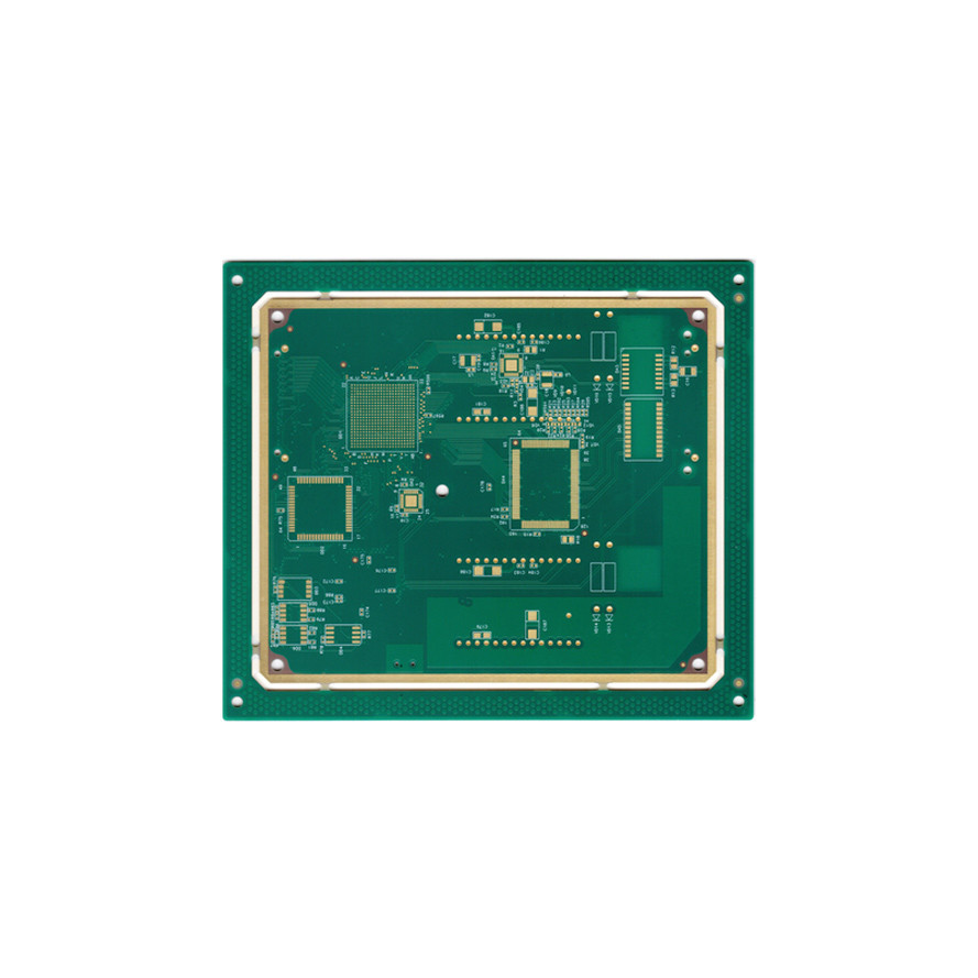
Cadence Allegro Assembly Languages PCB Prototype Service Bom Management
Introdution to our PCBs
PCB characteristics:
1. High wiring density, small size and light weight, which is conducive to the miniaturization of electronic equipment.
2. Due to the repeatability and consistency of the graphics, errors in wiring and assembly are reduced, and equipment maintenance, debugging and inspection time are saved.
3. It is conducive to mechanized and automated production, improving labor productivity and reducing the cost of electronic equipment.
4. The design can be standardized and easy to exchange. PCB is the abbreviation of Printed Circuit Board, translated into Chinese called printed circuit board, because it is made by electronic printing, so it is called "printed" circuit board. PCB is an important electronic component in the electronics industry, a support for electronic components, and a carrier for electrical connection of electronic components. PCB has been widely used in the manufacture of electronic products. why it is widely used.
PCB prototype service Capacities and Technical Specification
| NO. | Items | Capabilities |
| 1 | Layers | 2-68L |
| 2 | Maximum machining size | 600mm*1200mm |
| 3 | Board thickness | 0.2mm-6.5mm |
| 4 | Copper thickness | 0.5oz-28oz |
| 5 | Min trace/space | 2.0mil/2.0mil |
| 6 | Minimum finished aperture | 0. 10mm |
| 7 | Maximum thickness to diameter ratio | 15:1 |
| 8 | Via treatment | Via, blind&buried via, via in pad, Copper in via … |
| 9 | Surface finish/treatment | HASL/HASL lead free, Chemical tin, Chemical Gold, Immersion gold Inmersion Silver/Gold, Osp, Gold Plating |
| 10 | Base Material | FR408 FR408HR, PCL-370HR;IT180A, Megtron 6(Panasonic);Rogers4350, Rogers4003, RO3003, Rogers/Taconic/Arlon/Nelco laminate with FR-4 material(including partial Ro4350B hybrid laminating with FR-4) |
| 11 | Solder mask color | Green.Black.Red.Yellow.White.Blue.Purple.Matte Green. Matte Black |
| 12 | Testing Service | AOI, X-Ray, Flying-Probe, Function Test, First Article Tester |
| 13 | Profiling Punching | Routing,V-CUT,Beveling |
| 14 | Bow&twist | ≤0.5% |
| 15 | HDI type | 1+n+1,2+n+2,3+n+3 |
| 16 | Min mechanical aperture | 0.1mm |
| 17 | Min laser aperture | 0.075mm |
PCBA Capabilities
Briefly Introduce Our Strength
1. Born from technology, we understand R&D needs.
2. Break through the barriers from design to production.
3. Quality traceable.
4. Fast and on time delivery.
Medical equipment
Electronics make a major contribution to health - the nursing industry, as diagnostic, monitoring and therapeutic equipment. As the development of electronics becomes more efficient and dense, the medical applications of these electronic devices continue to grow, leading to endless new possibilities.At the heart of these medical devices is the PCB prototype service. PCBs in the medical industry are highly specialized to accommodate the unique constraints of medical devices. In many medical applications, small packages are required to meet the size requirements for implants or emergency room monitors. Therefore, medical PCBs tend to be specialty high-density interconnect prototype PCBs, also known as HDI PCBs. Medical PCBs can also be made with flexible substrates that allow PCB prototype service to bend during use, which is essential for both internal and external medical devices.
1. Monitors: Personal and healthcare monitors, including blood glucose monitors, heart rate and blood pressure monitors, and more.
2. Scanning Technology: CT scanners and ultrasound technology typically use PCB prototype service.
3. Control System: The device controls the infusion, flow rate and distribution are electronically controlled.
4. Internal Devices: Pacemakers and similar internal medical devices keep patients healthy and are operated by a central micro-PCB.
![]()
![]()
![]()
![]()
![]()
![]()
![]()
FAQ
| Q: What is needed for PCB & PCBA quotation? CESGATE: For PCB: Gerber file and technic requirements(material,size, surface finish treatment, copper thickness,board thickness) and quantity you need. For PCBA: Files mentioned above, BOM, pick and place file. |
| Q: What modes of transport are there? CESGATE: Usually includes express, air shipment, rail shipment and sea shipment. |
| Q: Can we inspect quality during production? CESGATE: Yes, we are open and transparent on each production process with nothing to hide. We welcome customer inspect our production process and check in house. |
| Q: Can you give us a preferential discount? CESGATE: Of course, we will offer a preferential discount for your large orders and confirm the order quickly. |
| Q: Why choose us? CESGATE: Professional and experienced R&D team. Advanced production equipment, scientific and reasonable process flow. Reliable and strict quality control system. We test all our products before shipment to make sure everything is in perfect condition. |
| Q: What are the types of solder mask? CESGATE: There are traditional epoxy resin IR baking type, UV curing type, Liquid Photo Imageable Solder Mask and Dry film solder mask. Currently, the liquid solder mask is the main type. |