

| Place of Origin: | China |
|---|---|
| Brand Name: | CESGATE |
| Certification: | UL, IATF16949, ISO9001 |
| Model Number: | NA |
| Minimum Order Quantity: | 1PCS( NO MOQ) |
| Price: | Negotiable (Depends on your GERBER and BOM) |
| Packaging Details: | PCB: Vacuum Packing / PCBA: ESD Packing |
| Delivery Time: | 3-7 working days |
| Payment Terms: | T/T, L/C |
| Supply Ability: | 13kk soldering spot/day |
| Product Name: | Rogers Fr4 Copper Quick Turn PCB Assembly Service Board To Board Connector | Feature: | Rogers Fr4 |
|---|---|---|---|
| Speed: | 0.15sec/chip, 0.7sec/QFP | Board Thickness: | 0.2mm-6.5mm |
| High-end Equipment: | FUJI NXT3/XPF Laminator | Shape: | Retangular/Round/Slots/Cutouts/Complex/Irregular |
| Solder Type: | Water Soluble Solder Paste,Leaded And Lead-Free | Surface Treatment: | OSP ,Immersion Gold, Immersion Tin ,Immersion Ag |
| High Light: | Rogers 4003 PCB Assembly Service,IATF16949 PCB Assembly Service |
||
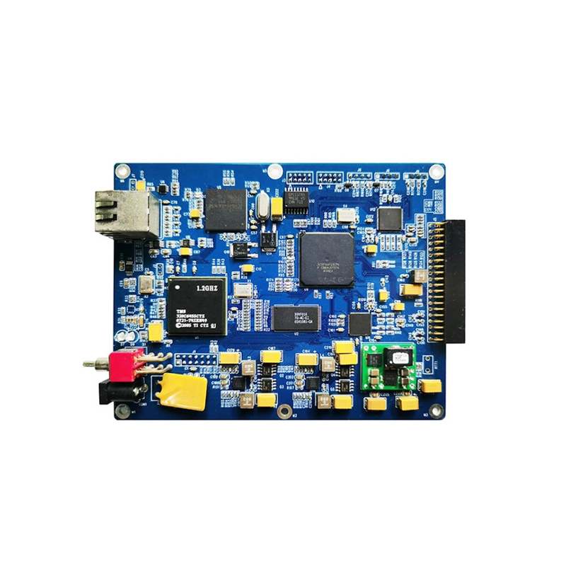
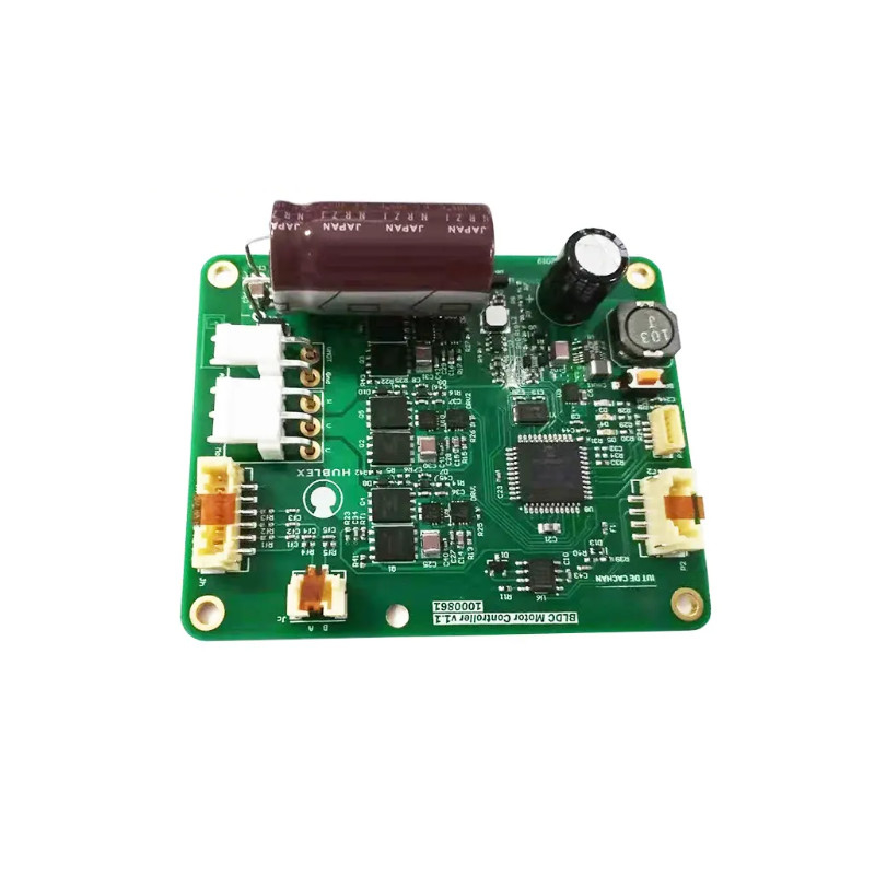
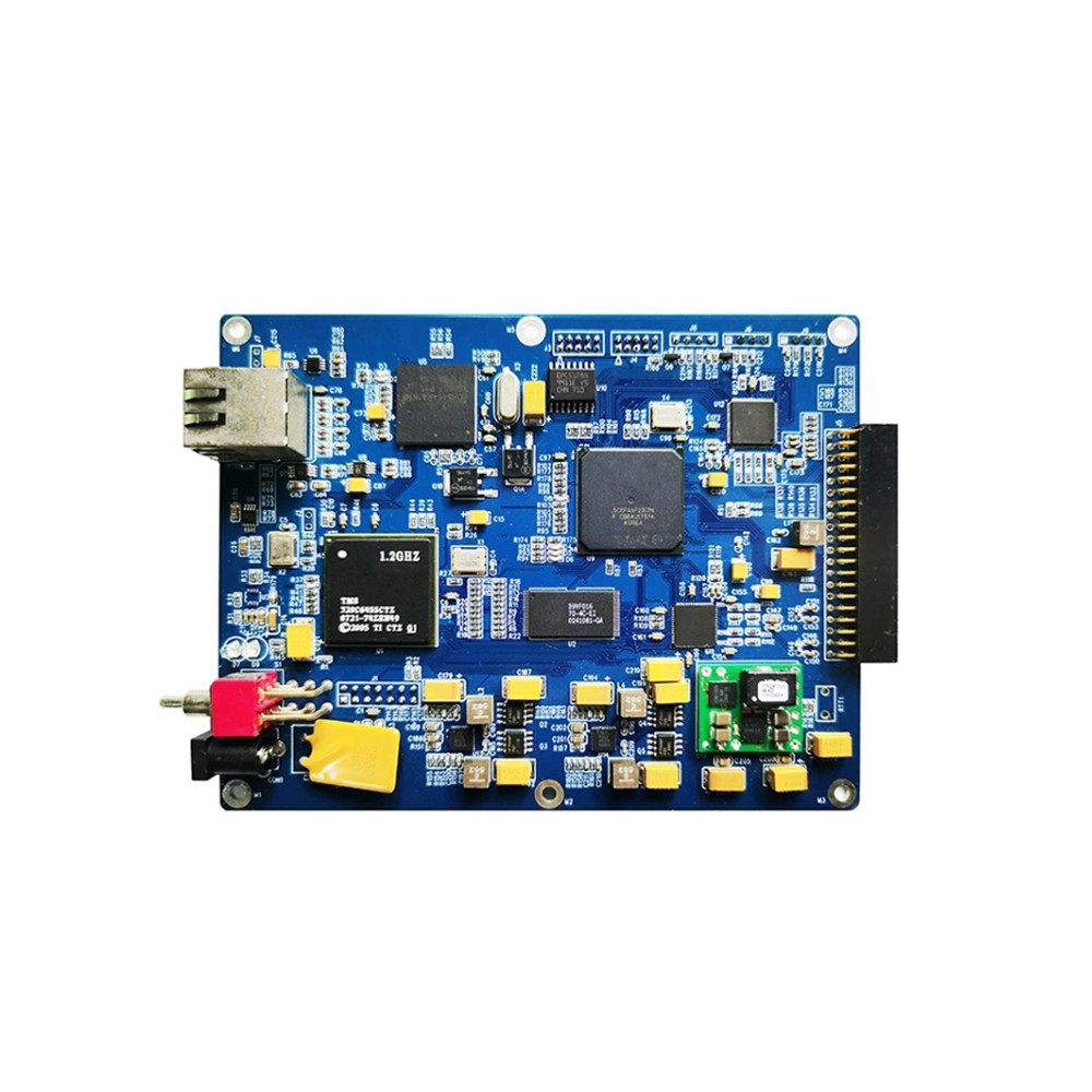
Rogers Fr4 Copper Quick Turn PCB Assembly Service Board To Board Connector
Solder resist application in PCB assembly service
Areas that should not be soldered may be covered with solder resist (solder mask). The solder mask is what gives PCBs their characteristic green color, although it is also available in several other colors, such as red, blue, purple, yellow, black and white. One of the most common solder resists used today is called "LPI" (liquid photoimageable solder mask).A photo-sensitive coating is applied to the surface of the PWB in PCB assembly, then exposed to light through the solder mask image film, and finally developed where the unexposed areas are washed away. Dry film solder mask is similar to the dry film used to image the PWB for plating or etching. After being laminated to the PWB surface it is imaged and developed as LPI. Once but no longer commonly used, because of its low accuracy and resolution, is to screen print epoxy ink. In addition to repelling solder, solder resist also provides protection from the environment to the copper that would otherwise be exposed.
![]()
Often encountered materials in PCB assembly service:
Specification
| NO. | Items | Capabilities |
| 1 | Layers | 2-68L |
| 2 | Maximum machining size | 600mm*1200mm |
| 3 | Board thickness | 0.2mm-6.5mm |
| 4 | Copper thickness | 0.5oz-28oz |
| 5 | Min trace/space | 2.0mil/2.0mil |
| 6 | Minimum finished aperture | 0. 10mm |
| 7 | Maximum thickness to diameter ratio | 15:1 |
| 8 | Via treatment | Via, blind&buried via, via in pad, Copper in via … |
| 9 | Surface finish/treatment | HASL/HASL lead free, Chemical tin, Chemical Gold, Immersion gold Inmersion Silver/Gold, Osp, Gold Plating |
| 10 | Base Material | FR408 FR408HR, PCL-370HR;IT180A, Megtron 6(Panasonic);Rogers4350, Rogers4003, RO3003, Rogers/Taconic/Arlon/Nelco laminate with FR-4 material(including partial Ro4350B hybrid laminating with FR-4) |
| 11 | Solder mask color | Green.Black.Red.Yellow.White.Blue.Purple.Matte Green. Matte Black |
| 12 | Testing Service | AOI, X-Ray, Flying-Probe, Function Test, First Article Tester |
| 13 | Profiling Punching | Routing,V-CUT,Beveling |
| 14 | Bow&twist | ≤0.5% |
| 15 | HDI type | 1+n+1,2+n+2,3+n+3 |
| 16 | Min mechanical aperture | 0.1mm |
| 17 | Min laser aperture | 0.075mm |
What CESGATE provide?
1. 7/24 Sales and technical support
2. Felxible payment methods and negotiable payment terms
3. Both samples and bulk orders are supported
4. More than 10 years overseas export experience, flexible handling of transportation and customs clearance issues
![]()
![]()
![]()
![]()
FAQ
|
Q: How long is the shelf life of the PCB board and how should it be stored? |
|
Q: How about the shipping cost? |
| Q: What are the types of solder mask? CESGATE: There are traditional epoxy resin IR baking type, UV curing type, Liquid Photo Imageable Solder Mask and Dry film solder mask. Currently, the liquid solder mask is the main type. |
| Q: Why choose us? CESGATE: Professional and experienced R&D team. Advanced production equipment, scientific and reasonable process flow. Reliable and strict quality control system. We test all our products before shipment to make sure everything is in perfect condition. |