


| Place of Origin: | China |
|---|---|
| Brand Name: | CESGATE |
| Certification: | UL, IATF16949, ISO9001 |
| Model Number: | NA |
| Minimum Order Quantity: | 1PCS( NO MOQ) |
| Price: | Negotiable (Depends on your GERBER and BOM) |
| Packaging Details: | PCB: Vacuum Packing / PCBA: ESD Packing |
| Delivery Time: | 3-7 working days |
| Payment Terms: | T/T, L/C |
| Supply Ability: | 13kk soldering spot/day |
| Product Name: | ISO9001 SMD ICs Roger Turnkey Soldering Pads PCB Assembly Service Rigid Fr4 | Feature: | Soldering Pads |
|---|---|---|---|
| Base Material: | FR4, FR4,Rogers,custom | Board Thickness: | 0.2mm-6.5mm |
| High-end Equipment: | FUJI NXT3/XPF Laminator | Max Board Size: | 680*550mm Smallest:0.25"*0.25" |
| Surface Finishing:: | ENIG,HASL,OSP,ENEPIG,Flash Gold | Surface Treatment: | OSP ,Immersion Gold, Immersion Tin ,Immersion Ag |
| Highlight: | Easyeda Designer PCB Assembly Service,OSP PCB Assembly Service |
||
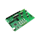
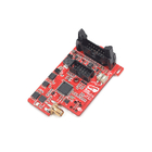
ISO9001 SMD ICs Roger Turnkey Soldering Pads PCB Assembly Service Rigid Fr4
What is a Printed Circuit Board (PCB)
Printed circuit board, also known as printed circuit board, printed circuit board, often used in English abbreviations are PCB (Printed circuit board) or PWB (Printed wire board). PCB is the base plate used to assemble electronic components, and it is also the "mother of electronic products". It is a very important electronic component and a support for electronic components. Mainly through the metal copper foil circuits on the board, through the design of each layer to connect and conduct related components, to achieve a complete product that operates effectively.
Before the early PCB assembly service appeared, the various components of electronic products were connected by wires to form a complete path. Later, in order to simplify the manufacturing process of electronic products and reduce the cost, the circuit was developed by printing, and the copper foil on the substrate was used to replace the original wire connection, thereby improving the production efficiency.
The various components are mainly connected through the metal copper foil circuits on the board. By designing each layer to connect and conduct related components, a complete product that operates effectively is achieved.
![]()
Advantages and disadvantages of Blind and buried vias
Blind and buried vias can help you to meet the high density constraints of lines and pads on a typical design without increasing the overall layer count or your board size.The vias also help you manage the printed circuit board aspect ratio and limit the change of break out.
Cost is still the main issue with boards using blind and buried viasin PCB assembly service, compared to the boards using standard through hole vias. The high cost is due to the increasing complexity of the board and more steps in the manufacturing process. At the same time, testing and precision checks are made more frequently.Venture engineers can look at your engineering requirements, space needs and the functionality of your PCB to help you reduce costs with buried and/or blind vias.
Specification
| NO. | Items | Capabilities |
| 1 | Layers | 2-68L |
| 2 | Maximum machining size | 600mm*1200mm |
| 3 | Board thickness | 0.2mm-6.5mm |
| 4 | Copper thickness | 0.5oz-28oz |
| 5 | Min trace/space | 2.0mil/2.0mil |
| 6 | Minimum finished aperture | 0. 10mm |
| 7 | Maximum thickness to diameter ratio | 15:1 |
| 8 | Via treatment | Via, blind&buried via, via in pad, Copper in via … |
| 9 | Surface finish/treatment | HASL/HASL lead free, Chemical tin, Chemical Gold, Immersion gold Inmersion Silver/Gold, Osp, Gold Plating |
| 10 | Base Material | FR408 FR408HR, PCL-370HR;IT180A, Megtron 6(Panasonic);Rogers4350, Rogers4003, RO3003, Rogers/Taconic/Arlon/Nelco laminate with FR-4 material(including partial Ro4350B hybrid laminating with FR-4) |
| 11 | Solder mask color | Green.Black.Red.Yellow.White.Blue.Purple.Matte Green. Matte Black |
| 12 | Testing Service | AOI, X-Ray, Flying-Probe, Function Test, First Article Tester |
| 13 | Profiling Punching | Routing,V-CUT,Beveling |
| 14 | Bow&twist | ≤0.5% |
| 15 | HDI type | 1+n+1,2+n+2,3+n+3 |
| 16 | Min mechanical aperture | 0.1mm |
| 17 | Min laser aperture | 0.075mm |
![]()
![]()
![]()
![]()
Who are we?
Welcome to Chengdu Cesgate Technology Co., Ltd
We can provide one-stop service:
PCB circuit boards+PCB assembly service
E-test.
Electronic components purchasing.
PCB assembly service: available on SMT, BGA, DIP.
PCBA function test.
Enclosure assembly.
FAQ
|
Q: How can we guarantee quality? |
|
Q: Why should we buy from CESGATE? |
| Q: How can we guarantee quality? CESGATE: Always a pre-production sample before mass production; Always final Inspection and test report before shipment; |
| Q: What does CESGATE need for a customized PCB order? CESGATE: When you place a PCB order, the customers need to provide Gerber or pcb file. If you do not have the file in the correct format, you can send all the details related to the products. |


