

| Place of Origin: | China |
|---|---|
| Brand Name: | CESGATE |
| Certification: | UL, IATF16949, ISO9001 |
| Model Number: | NA |
| Minimum Order Quantity: | 1PCS( NO MOQ) |
| Price: | Negotiable (Depends on your GERBER and BOM) |
| Packaging Details: | PCB: Vacuum Packing / PCBA: ESD Packing |
| Delivery Time: | 3-7 working days |
| Payment Terms: | T/T, L/C |
| Supply Ability: | 13kk soldering spot/day |
| Product Name: | Quick Turn Through Hole Printing PCB Assembly Service SMT Soldering | Feature: | Quick Turn |
|---|---|---|---|
| Min Package: | 03015 | High-end Equipment: | FUJI NXT3/XPF Laminator |
| Test: | AOI/ X-Ray/Flying-Probe/Function Test | Base Material: | FR-4, Rogers, Aluminum, CEM-1 OR FR-4, FR4/FR1/ FR2/ FR3/ CEM1/ CEM3/ROGERS/ARLON/ISOLA |
| Min. Hole Size: | 0.2mm, 4mil-laser Drill, 6mil, 0.1mm-1mm, 0.15mm | Layer: | 2-68layers |
| Highlight: | Printing PCB Assembly Service,PCB Assembly Service SMT Soldering |
||
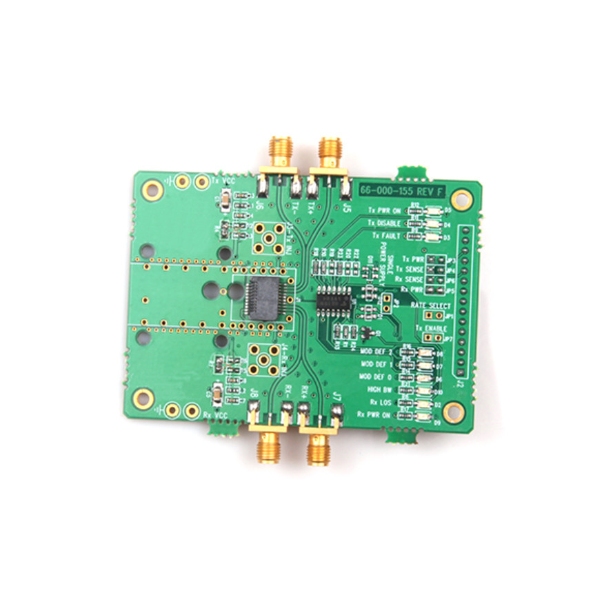
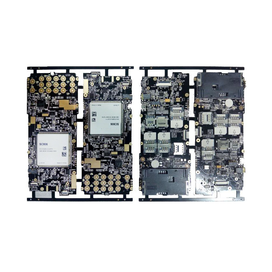
Quick Turn Through Hole Printing PCB Assembly Service SMT Soldering
We handle all types of PCB assembly projects with any quantity especially small batch assembly and low volume PCB assembly, from basic through-hole PCB assembly technology to standard surface mount assembly (SMT PCB assembly and PCB SMT assembly), mixed assembly, kit assembly to ultra-fine pitch BGA assembly.Our PCB types for our custom PCB assembly include: rigid PCB, Metal Core PCB, flex PCB and rigid flex PCB..etc.
![]()
![]()
PCB characteristics:
1. High wiring density, small size and light weight, which is conducive to the miniaturization of electronic equipment.
2. Due to the repeatability and consistency of the graphics, errors in wiring and Turnkey PCB Assembly are reduced, and equipment maintenance, debugging and inspection time are saved.
3. It is conducive to mechanized and automated production, improving labor productivity and reducing the cost of electronic equipment.
4. The design can be standardized and easy to exchange. PCB is the abbreviation of Printed Circuit Board, translated into Chinese called printed circuit board, because it is made by electronic printing, so it is called "printed" circuit board. PCB is an important electronic component in the electronics industry, a support for electronic components, and a carrier for electrical connection of electronic components. PCB has been widely used in the manufacture of electronic products.
Applications:
Consumer electronics are devices we use every day, such as smartphones or computers. Even the latest model refrigerators often contain electronic components. Each of these devices is a PCB.
Since these consumer electronics products are manufactured in high volumes, the number of PCBs that control them must be equal. These high-volume PCBs have lower unit costs, making the price of the final product relatively small. The challenge is to maintain the uniformity and quality of these PCBs, which is why PCB manufacturers must adhere to strict industry standards and quality control measures to ensure that each consumer's electronics function as expected.
PCBs are widely used in consumer electronics. Here are some common uses of PCBs in consumer electronics:
1. Mobile Devices: Smartphones and tablets are at the heart of our daily work, our GPS alarm clocks.
2. Computer Electronics: Both desktop and laptop computers contain the PCB at their core, as do the screen and the peripherals associated with it.
3. Recording Devices: Camcorders, digital cameras, microphones, and other recording devices all rely on their internal PCBs to function.
4. Entertainment System: Everything in a home entertainment system, from DVD players and video game consoles to TVs and audio equipment.
5. Home Appliances: Almost all modern appliances run using electronic components: alarm clocks, microwaves, refrigerators, coffee makers, etc.
Specification
| NO. | Items | Capabilities |
| 1 | Layers | 2-68L |
| 2 | Maximum machining size | 600mm*1200mm |
| 3 | Board thickness | 0.2mm-6.5mm |
| 4 | Copper thickness | 0.5oz-28oz |
| 5 | Min trace/space | 2.0mil/2.0mil |
| 6 | Minimum finished aperture | 0. 10mm |
| 7 | Maximum thickness to diameter ratio | 15:1 |
| 8 | Via treatment | Via, blind&buried via, via in pad, Copper in via … |
| 9 | Surface finish/treatment | HASL/HASL lead free, Chemical tin, Chemical Gold, Immersion gold Inmersion Silver/Gold, Osp, Gold Plating |
| 10 | Base Material | FR408 FR408HR, PCL-370HR;IT180A, Megtron 6(Panasonic);Rogers4350, Rogers4003, RO3003, Rogers/Taconic/Arlon/Nelco laminate with FR-4 material(including partial Ro4350B hybrid laminating with FR-4) |
| 11 | Solder mask color | Green.Black.Red.Yellow.White.Blue.Purple.Matte Green. Matte Black |
| 12 | Testing Service | AOI, X-Ray, Flying-Probe, Function Test, First Article Tester |
| 13 | Profiling Punching | Routing,V-CUT,Beveling |
| 14 | Bow&twist | ≤0.5% |
| 15 | HDI type | 1+n+1,2+n+2,3+n+3 |
| 16 | Min mechanical aperture | 0.1mm |
| 17 | Min laser aperture | 0.075mm |
Company Profile
CESGATE is a team with more than 10 years experience in the field. We owns abundant experiences for serving overseas customers from industrial automatic control, communication, medical, Auto and consumer electronics,etc. We test our product strictly to guarantee the quality to our customers. We accumulate high reputation during our cooperation.You will achieve following value-added services when you cooperate with us:
One-stop PCB/Turnkey PCB Assembly Service
Optimizing your PCB design during production
Satisfied quality with competitive prices
Instant response in both quotation and delivery
Increase your business with our powerful support
![]()
![]()
![]()
![]()
FAQ
| Q: What is your delivery date? CESGATE: The general sample delivery time is 6 working days for single and double-sided boards, 7 working days for 4-layer boards, and an additional working day for every 2 layers. However, if there are special processes, additional working days will be added according to the situation. Generally, the delivery time for mass production is 10 working days for single and double-sided panels, and 15 working days for multi-layer panels. However, if there is a special process or more than a certain number of working days, the working days will be additionally increased according to the situation; you can also pay the urgent fee to shorten the number of days, please contact Contact the business specially proposed, depending on the individual situation to provide expedited days. |
| Q: What is the difference between the HDI board and the general circuit board? CESGATE: Most of HDI use laser to form holes, while general circuit boards only use mechanical drilling, and HDI boards are manufactured by the build-up method (Build Up), so more layers will be added, while general circuit boards are only added once. |
| Q: What are the types of solder mask? CESGATE: There are traditional epoxy resin IR baking type, UV curing type, Liquid Photo Imageable Solder Mask and Dry film solder mask. Currently, the liquid solder mask is the main type. |
| Q: What are the common substrates of CESGATE? A:Tg-140: ISOLA FR402 / NAN-YA NP-140 Tg-150: ISOLA IS400 / NAN-YA NP-155 Tg-170~180: ISOLA 370HR / NPN-YA / NAN-YA NP-175F |