

| Place of Origin: | China |
|---|---|
| Brand Name: | CESGATE |
| Certification: | UL, IATF16949, ISO9001 |
| Model Number: | NA |
| Minimum Order Quantity: | 1PCS( NO MOQ) |
| Price: | Negotiable (Depends on your GERBER and BOM) |
| Packaging Details: | PCB: Vacuum Packing / PCBA: ESD Packing |
| Delivery Time: | 3-7 working days |
| Payment Terms: | T/T, L/C |
| Supply Ability: | 13kk soldering spot/day |
| Product Name: | Aluminium Circuit Board PCB Assembly Service Rogers Fr4 Prototype Soldering | Feature: | Rogers Fr4 |
|---|---|---|---|
| Maximum Thickness To Diameter Ratio: | 15:1 | Service: | One-stop Turnkey Service |
| High-end Equipment: | FUJI NXT3/XPF Laminator | Material: | FR4/M4/M6/Rogers/TU872/IT968 |
| Test: | AOI/SPI/XRAY/First Article Inspection | Min Laser Aperture: | 0.075mm |
| High Light: | Uyue 946c PCB Assembly Service,FR408 PCB Assembly Service |
||
Aluminium Circuit Board PCB Assembly Service Rogers Fr4 Prototype Soldering
In PCB assembly service,The first step is to replicate the pattern in the fabricator's CAM system on a protective mask on the copper foil PCB layers. Subsequent etching removes the unwanted copper unprotected by the mask. (Alternatively, a conductive ink can be ink-jetted on a blank (non-conductive) board. This technique is also used in the manufacture of hybrid circuits.)
The method chosen depends on the number of boards to be produced and the required resolution.
![]()
Lamination in PCB assembly service
INATIONMulti-layer printed circuit boards have trace layers inside the board. This is achieved by laminating a stack of materials in a press by applying pressure and heat for a period of time. This results in an inseparable one piece product. For example, a four-layer PCB assembly service can be fabricated by starting from a two-sided copper-clad laminate, etch the circuitry on both sides, then laminate to the top and bottom pre-preg and copper foil. It is then drilled, plated, and etched again to get traces on top and bottom layers.
The inner layers are given a complete machine inspection before lamination because mistakes cannot be corrected afterwards. Automatic optical inspection (AOI) machines compare an image of the board with the digital image generated from the original design data. Automated Optical Shaping (AOS) machines can then add missing copper or remove excess copper using a laser, reducing the number of PCBs that have to be discarded. PCB tracks can have a width of just 10 micrometers.
Specification
| NO. | Items | Capabilities |
| 1 | Layers | 2-68L |
| 2 | Maximum machining size | 600mm*1200mm |
| 3 | Board thickness | 0.2mm-6.5mm |
| 4 | Copper thickness | 0.5oz-28oz |
| 5 | Min trace/space | 2.0mil/2.0mil |
| 6 | Minimum finished aperture | 0. 10mm |
| 7 | Maximum thickness to diameter ratio | 15:1 |
| 8 | Via treatment | Via, blind&buried via, via in pad, Copper in via … |
| 9 | Surface finish/treatment | HASL/HASL lead free, Chemical tin, Chemical Gold, Immersion gold Inmersion Silver/Gold, Osp, Gold Plating |
| 10 | Base Material | FR408 FR408HR, PCL-370HR;IT180A, Megtron 6(Panasonic);Rogers4350, Rogers4003, RO3003, Rogers/Taconic/Arlon/Nelco laminate with FR-4 material(including partial Ro4350B hybrid laminating with FR-4) |
| 11 | Solder mask color | Green.Black.Red.Yellow.White.Blue.Purple.Matte Green. Matte Black |
| 12 | Testing Service | AOI, X-Ray, Flying-Probe, Function Test, First Article Tester |
| 13 | Profiling Punching | Routing,V-CUT,Beveling |
| 14 | Bow&twist | ≤0.5% |
| 15 | HDI type | 1+n+1,2+n+2,3+n+3 |
| 16 | Min mechanical aperture | 0.1mm |
| 17 | Min laser aperture | 0.075mm |
Strengths of CESGATE
1. Provide full BOM component supply and part selection
2. From the original factory and the first-level agents, the original authentic guarantee
3. More than 50,000 kinds of components are always in stock
4. Customers can buy on demand, no need to buy the whole package
5. Nitrogen gas reflow soldering technology for SMT.
6. High Standard SMT&Solder Assembly Line
7. High density interconnected board placement technology capacity.
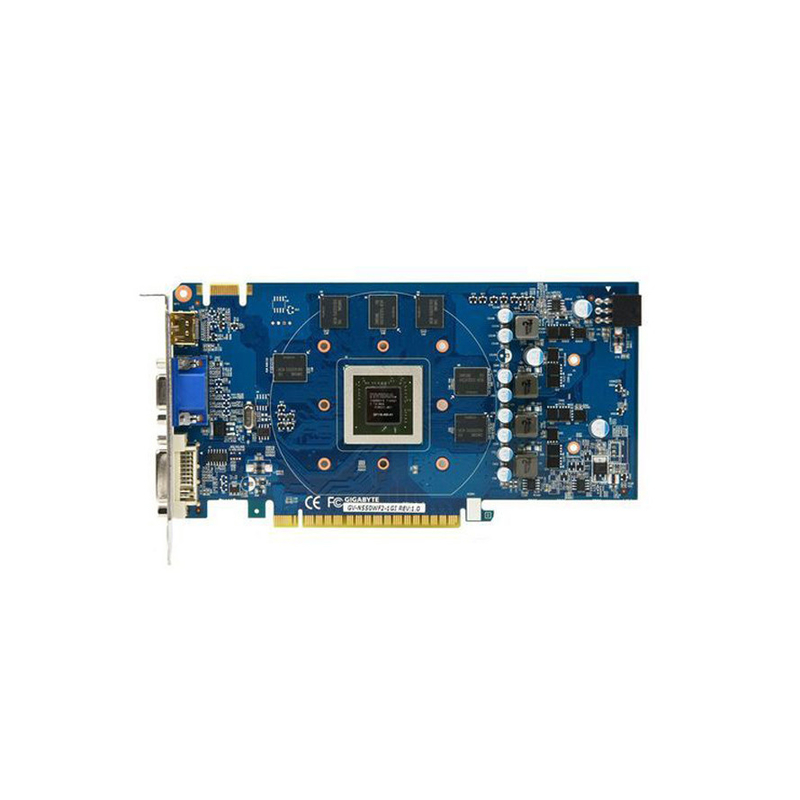
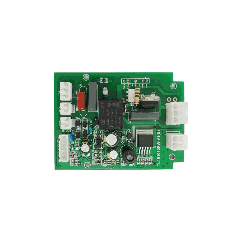
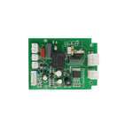
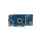
![]()
![]()
![]()
![]()
FAQ
| Q: What does CESGATE need for a customized PCB order? CESGATE: When you place a PCB order, the customers need to provide Gerber or pcb file. If you do not have the file in the correct format, you can send all the details related to the products. |
| Q: What is needed for PCB & PCB Assembly quotation? CESGATE: For PCB: Gerber file and technic requirements(material,size, surface finish treatment, copper thickness,board thickness) and quantity you need. For PCB Assembly: Files mentioned above, BOM, pick and place file. |
| Q: What is your inspection policy? How do you control the quality? CESGATE: In order to ensure the quality of PCB products, flying probe inspection is usually used; electrical fixtures, automatic optical inspection (AOI), BGA parts x-ray inspection, first article inspection ( FAI) etc. |
| Q: IS PRODUCT PICTURES AND LABELS AVAILABLE? CESGATE: We will offer after you place an order or before shipment. |