


| Place of Origin: | China |
|---|---|
| Brand Name: | CESGATE |
| Certification: | UL, IATF16949, ISO9001 |
| Model Number: | NA |
| Minimum Order Quantity: | 1PCS( NO MOQ) |
| Price: | Negotiable (Depends on your GERBER and BOM) |
| Packaging Details: | PCB: Vacuum Packing / PCBA: ESD Packing |
| Delivery Time: | 3-7 working days |
| Payment Terms: | T/T, L/C |
| Supply Ability: | 13kk soldering spot/day |
| Product Name: | Rogers Fr4 PCB Assembly Service High Volume Audio Amplifier Circuit Board | Feature: | Rogers Fr4 |
|---|---|---|---|
| Min Package: | 03015 | Board Thickness: | 0.2mm-6.5mm |
| High-end Equipment: | FUJI NXT3/XPF Laminator | Shape: | Retangular/Round/Slots/Cutouts/Complex/Irregular |
| Max Board Size: | 680*550mm Smallest:0.25"*0.25" | Surface Treatment: | OSP ,Immersion Gold, Immersion Tin ,Immersion Ag |
| High Light: | Rogers Fr4 Pcb Components Assembly,High Volume PCB Assembly Service,UL Audio Amplifier Circuit Board |
||
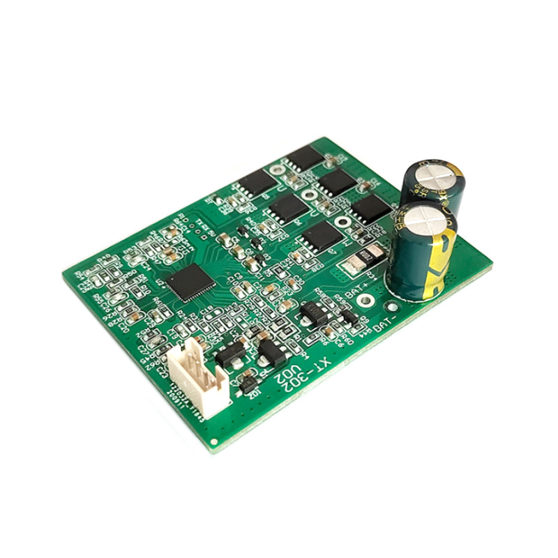
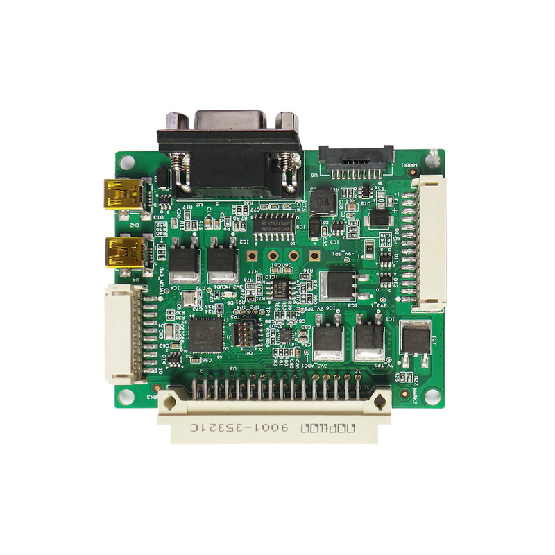
Rogers Fr4 PCB Assembly Service High Volume Audio Amplifier Circuit Board
Often encountered materials in PCB assembly service
![]()
PCB Process - Introduction to HDI
HDI (High Density Interconnect): High-density interconnection technology, mainly using micro-blind / buried vias (blind / buried vias), a technology that makes PCB prototype service distribution density higher. The advantage is that it can greatly increase the usable area of the PCB circuit board, making the product as miniaturized as possible in PCB assembly service. However, due to the increase in line distribution density, it is impossible to use traditional drilling methods to drill through holes, and some of the via holes must be drilled with laser drilling to form blind holes, or cooperate with inner-layer buried vias to interconnect.
Generally speaking, HDI circuit boards use the build-up method (Build Up), first do or press the inner layers, laser drilling and electroplating on the outer layer are completed, and then the outer layer is covered with an insulating layer (prepreg). ) and copper foil, and then repeat the outer layer circuit making, or continue to laser drill, and stack the layers outward one at a time.
Generally, the diameter of the laser drilling hole is designed to be 3 ~ 4 mil (about 0.076 ~ 0.1 mm), and the insulation thickness between each laser drilling layer is about 3 mil. Due to the use of laser drilling many times, the key to the quality of the HDI circuit board is the hole pattern after laser drilling and whether the hole can be evenly filled after the subsequent electroplating and filling.
The following are examples of HDI board types. The pink holes in the picture are blind holes, which are made by laser drilling, and the diameter is usually 3 to 4 mil; the yellow holes are buried holes, which are made by mechanical drilling, and the diameter is at least 6 mil (0.15 mm).
Specification
| NO. | Items | Capabilities |
| 1 | Layers | 2-68L |
| 2 | Maximum machining size | 600mm*1200mm |
| 3 | Board thickness | 0.2mm-6.5mm |
| 4 | Copper thickness | 0.5oz-28oz |
| 5 | Min trace/space | 2.0mil/2.0mil |
| 6 | Minimum finished aperture | 0. 10mm |
| 7 | Maximum thickness to diameter ratio | 15:1 |
| 8 | Via treatment | Via, blind&buried via, via in pad, Copper in via … |
| 9 | Surface finish/treatment | HASL/HASL lead free, Chemical tin, Chemical Gold, Immersion gold Inmersion Silver/Gold, Osp, Gold Plating |
| 10 | Base Material | FR408 FR408HR, PCL-370HR;IT180A, Megtron 6(Panasonic);Rogers4350, Rogers4003, RO3003, Rogers/Taconic/Arlon/Nelco laminate with FR-4 material(including partial Ro4350B hybrid laminating with FR-4) |
| 11 | Solder mask color | Green.Black.Red.Yellow.White.Blue.Purple.Matte Green. Matte Black |
| 12 | Testing Service | AOI, X-Ray, Flying-Probe, Function Test, First Article Tester |
| 13 | Profiling Punching | Routing,V-CUT,Beveling |
| 14 | Bow&twist | ≤0.5% |
| 15 | HDI type | 1+n+1,2+n+2,3+n+3 |
| 16 | Min mechanical aperture | 0.1mm |
| 17 | Min laser aperture | 0.075mm |
Company Profile
CESGATE with manufacturing PCB assembly service for over 10 years. During this time technology has moved forward at an amazing pace. By keeping abreast of technology, we can populate any PCB with SMD and conventional Components, single or double sided, one layer, to multilayer to any of your requirements and configurations.Our main services include PCB assembly (Electronic assembly), component procurement and PCB fabrication from quick turn, sample run to volume production.
Our customers are who of the Medical, Instrumentation, Intelligent home, Automotive, Consumer electronics industry and Robotics industries.
Full range of PCB manufacturing and assembly services to fit all of your printed circuit board needs.
![]()
![]()
![]()
![]()
FAQ
|
Q: Do you have any other services? |
|
Q: The Wire Bonding process is required when the circuit board is printed. What should I pay attention to when making the circuit board? |
| Q: How can we guarantee quality? CESGATE: Always a pre-production sample before mass production; Always final Inspection and test report before shipment; |
| Q: Can we inspect quality during production? CESGATE: Yes, we are open and transparent on each production process with nothing to hide. We welcome customer inspect our production process and check in house.ty. |