

| Place of Origin: | China |
|---|---|
| Brand Name: | CESGATE |
| Certification: | ISO9001/ ISO14001 |
| Model Number: | NA |
| Minimum Order Quantity: | 1PCS( NO MOQ) |
| Price: | Negotiable (Depends on your GERBER and BOM) |
| Packaging Details: | PCB: Vacuum Packing / PCBA: ESD Packing |
| Delivery Time: | 1-30 working days |
| Payment Terms: | T/T, L/C |
| Supply Ability: | 30,000pcs/month |
| Features: | SMD/PCB | Product Name: | SMD Automation Manufacturing Fabrication PCB Prototype Service Customized Logo |
|---|---|---|---|
| Material: | Stainless Steel, Aluminum, Plastic, Brass, Copper Etc | Optional Service: | 3 4 5 6 Axis CNC Machining Service |
| Min. Line Spacing: | 4mil, 0.003", 0.1mm4mil), 0.1mm, 4/4mil(0.1/0.1mm) | Min. Line Width: | 4mil, 0.1mm, 0.1mm/4mi, 0.075mm/0.075mm(3mil/3mil), 3mi |
| Min. Hole Size: | 0.2mm, 8 Mil, 0.10mm, 3mil (0.075mm), 0.004" | MOQ: | Small Orders Accepted |
| High Light: | SMD PCB Prototype Service,6 Axis CNC Fabrication PCB Prototype,5 Axis CNC Fabrication PCB Prototype |
||
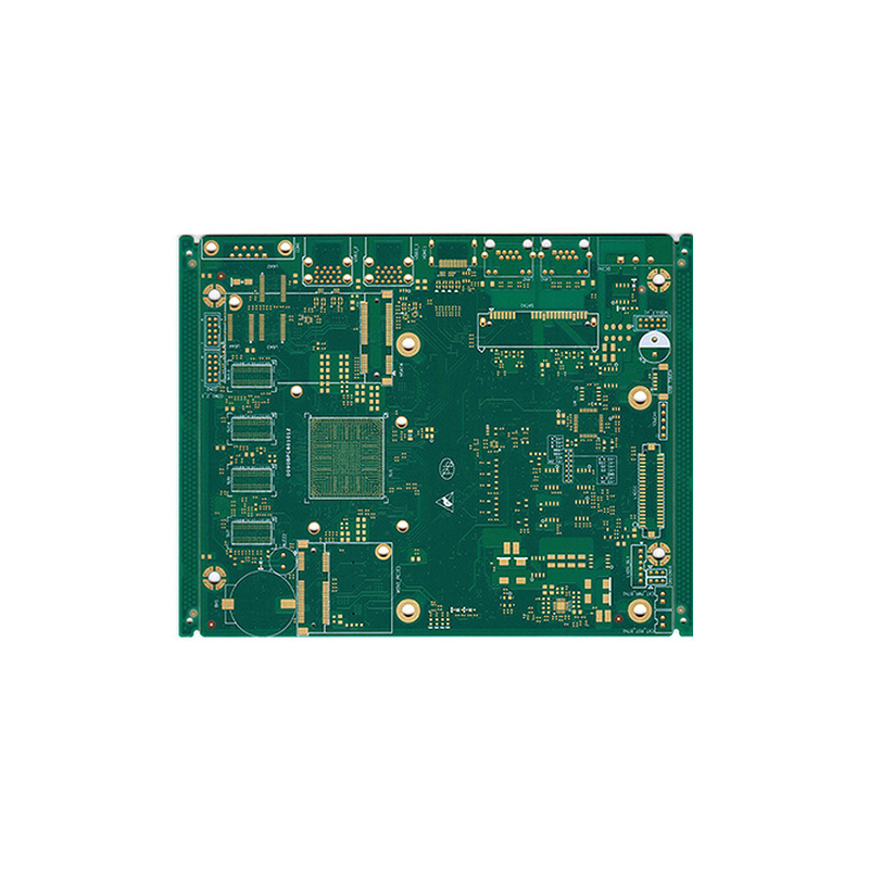
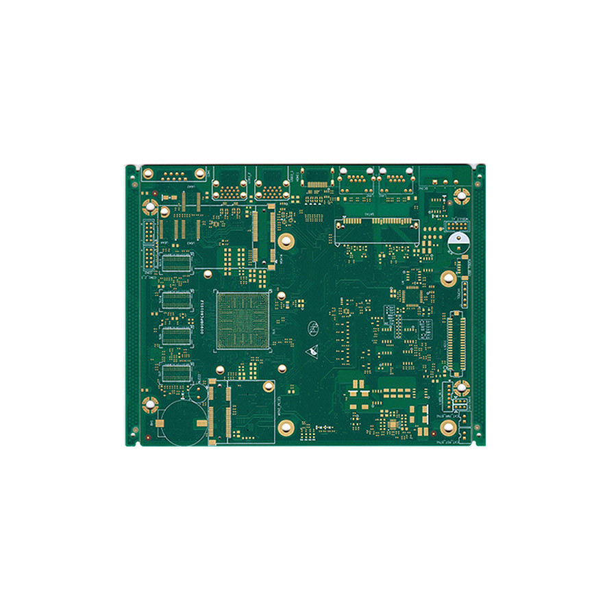
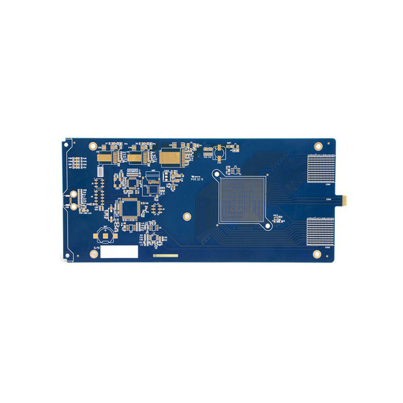
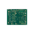
SMD Automation Manufacturing Fabrication PCB Prototype Service Customized Logo
Our Strengths
GESGATE is experienced in engineering, eliminate problems and traps before production. In the PCB industry for more than ten years, we build a standardized and rigorous process and system has been established to effectively reduce quality problems. We have professional PCB manufacturing, PCB Prototype service and component procurement team, providing one-stop service, saving time and effort. We can provide services such as fast delivery, minimum mount. We have expedited 8-hour delivery, with a 48-hour delivery rate of over 95% and 03015, 01005, 0201, 0402 in minimum mount. Actually we are experienced in engineering, eliminate problems and traps before production. We are professional PCB manufacturing, PCB Prototype services supplier and component procurement team, providing one-stop service, saving time and effort.
Our Production Lines
Our company currently has 7 wave soldering production lines and 10 post-DIP soldering lines. We can make special fixtures according to customer requirements and product conditions to ensure product reliability and effectively improve plug-in efficiency.
Our DIP post-welding personnel have rich experience, and have formulated detailed standardized operation guidelines and SOP operation instructions to meet the high-quality requirements of high-end customers.
PCB Prototype Service Capacities and Technical Specification
| NO. | Items | Capabilities |
| 1 | Layers | 2-68L |
| 2 | Maximum machining size | 600mm*1200mm |
| 3 | Board thickness | 0.2mm-6.5mm |
| 4 | Copper thickness | 0.5oz-28oz |
| 5 | Min trace/space | 2.0mil/2.0mil |
| 6 | Minimum finished aperture | 0. 10mm |
| 7 | Maximum thickness to diameter ratio | 15:1 |
| 8 | Via treatment | Via, blind&buried via, via in pad, Copper in via … |
| 9 | Surface finish/treatment | HASL/HASL lead free, Chemical tin, Chemical Gold, Immersion gold Inmersion Silver/Gold, Osp, Gold Plating |
| 10 | Base Material | FR408 FR408HR, PCL-370HR;IT180A, Megtron 6(Panasonic);Rogers4350, Rogers4003, RO3003, Rogers/Taconic/Arlon/Nelco laminate with FR-4 material(including partial Ro4350B hybrid laminating with FR-4) |
| 11 | Solder mask color | Green.Black.Red.Yellow.White.Blue.Purple.Matte Green. Matte Black |
| 12 | Testing Service | AOI, X-Ray, Flying-Probe, Function Test, First Article Tester |
| 13 | Profiling Punching | Routing,V-CUT,Beveling |
| 14 | Bow&twist | ≤0.5% |
| 15 | HDI type | 1+n+1,2+n+2,3+n+3 |
| 16 | Min mechanical aperture | 0.1mm |
| 17 | Min laser aperture | 0.075mm |
PCBA Capabilities
Company Descripiton
Producing a qualified product is crucial to CESGATE and to you. To ensure PCB Prototype service are compliant we use a number of inspection and Quality assurance procedures. Including Automatic Optical Inspection equipment and CAD software as well as continuous improvements. We are accredited to ISO9001:2015 as well as being a preferred supplier to many of our customers. With access to global suppliers, and distribution networks we can source parts for your assemblies as needed. Using our own in-house Stock and MRP system which links to our production data we are able to manage Inventory levels, lead times and buffer stocks to meet your deadlines.
![]()
![]()
![]()
![]()
![]()
![]()
![]()
FAQ
| Q: The Wire Bonding process is required when the circuit board is printed. What should I pay attention to when making the circuit board? CESGATE: When making circuit boards, the surface treatment options are mostly "nickel palladium gold ENEPIG" or "chemical gold ENIG". If the Al aluminum wire is used, the gold thickness is recommended to be 3μ”~5μ”, but if the Au gold wire is used, the gold thickness should preferably be more than 5μ”. |
| Q: The lead-free process is required when the circuit board is printed. What should I pay attention to when making the circuit board? CESGATE: The lead-free process during printing is higher than the temperature resistance requirements of the general process, and the temperature resistance requirements must be above 260 °C. Therefore, it is recommended to use a substrate above TG150 when selecting the substrate material. |
| Q: Can your company provide the serial number when making circuit board text? CESGATE: Serial numbers can be provided, and in addition to text serial numbers, QR-CODE can also be provided for customers to query. |
| Q: How long is the shelf life of the PCB board and how should it be stored? CESGATE: 25℃ / 60%RH is recommended when the PCB is stored. The plate itself has no shelf life, but if it exceeds three months, it needs to be baked to remove moisture and stress, and it should be used immediately after baking. It is recommended that the pieces should be loaded within 6 months of storage to reduce the phenomenon of rejection and explosion. |