
| Place of Origin: | China |
|---|---|
| Brand Name: | CESGATE |
| Certification: | ISO9001/ ISO14001 |
| Model Number: | NA |
| Minimum Order Quantity: | 1PCS( NO MOQ) |
| Price: | Negotiable (Depends on your GERBER and BOM) |
| Packaging Details: | PCB: Vacuum Packing / PCBA: ESD Packing |
| Delivery Time: | 1-30 working days |
| Payment Terms: | T/T, L/C |
| Supply Ability: | 30,000pcs/month |
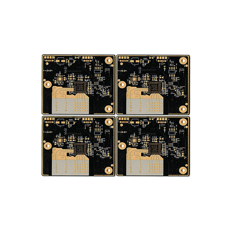
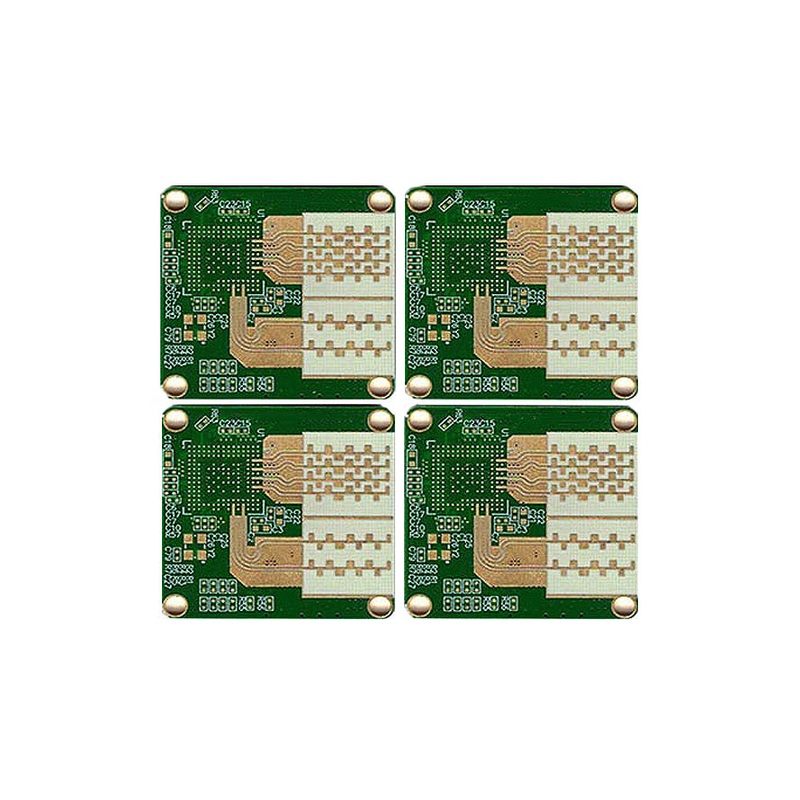
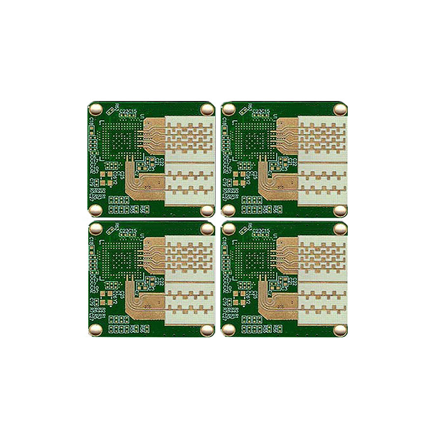
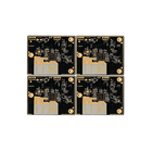
| Product Name: | Gold Impregnated One-Stop Oem Service High Frequency PCB SMT DIP OEM Electronic | Feature: | Gold Impregnated |
|---|---|---|---|
| Min. Line Width: | 0.2mm, 3mi, 0.075mm, 0.075mm/0.075mm(3mil/3mil), 0.1 0mm | Min. Hole Size: | 0.20mm, 0.1mm, 8 Mil, 0.254-0.40mm, 0.1mm-1mm |
| Surface Finishing: | HASL, OSP, ENIG, Immersion Gold, HASL Lead Free/OSP/Soft Gold/Hard Gold | Min Trace/gap: | 0.075mm Or 3mil |
| Copper Thickness: | 1oz, 1/2OZ 1OZ 2OZ 3OZ, As Your Request, 0.5-3.0 Oz, 1 Oz | Base Material: | FR4, Aluminum, Rogers, CEM-1, TG |
| High Light: | Gold Impregnated High Frequency PCB,Gold Impregnated pcb printed circuit board,pcb printed circuit board 0.075mm 3mil |
||
Gold Impregnated One-Stop Oem Service High Frequency PCB SMT DIP OEM Electronic
Plan your High Frequency PCB Design
You need to have a proper design for your High Frequency PCB before you start the actual PCB design. This is important to avoid setbacks or to have unexpected issues with your PCB.
What you need to do is to have a checklist if you are going to need during your PCB design. Among the key considerations that you need to look into include:
System organization which involves you having a visual representation of subcircuits interconnections.
Know the Signal Frequency of your PCB
Ensure that you have documented the power and voltage requirements for the ICs and if you will have to divide any power planes.
Check if you can accommodate the different signals, trace length as well as any controlled impedance.
At this stage, your manufacturer plays a vital role in ensuring that you understand what their minimum tolerance requirements are.
Also, you need to have a strategy that which will reduce the level of noise on your High Frequency PCB signals
Document all Your Board Stack Up Plan for Manufacturing
Once you have a plan of how you are going to design your PCB, you will have to document the requirements for your stack up layer.
You can consult with your manufacturer to determine the specifics for your PCBs.
This includes understanding the materials and the specific constraints for your PCB. You can either use FR-4, Nelco or Rodgers materials for your PCB.
You can have other strategies for your stack up such as having a signal layer which you can place next on an adjacent layer. This will offer signals that have an efficient return path.
You can also consider routing the High Frequency PCB signals which are on the inner layers of your PCB between planes.
This will offer to shield over any radiation that it emits externally.
Also, on your layer stack up, you may use many ground planes.
The purpose for this is to reduce your reference hinderance which in turn minimizes the effect of radiation on your circuit.
PCB Capacities and Technical Specification
| NO. | Items | Capabilities |
| 1 | Layers | 2-68L |
| 2 | Maximum machining size | 600mm*1200mm |
| 3 | Board thickness | 0.2mm-6.5mm |
| 4 | Copper thickness | 0.5oz-28oz |
| 5 | Min trace/space | 2.0mil/2.0mil |
| 6 | Minimum finished aperture | 0. 10mm |
| 7 | Maximum thickness to diameter ratio | 15:1 |
| 8 | Via treatment | Via, blind&buried via, via in pad, Copper in via … |
| 9 | Surface finish/treatment | HASL/HASL lead free, Chemical tin, Chemical Gold, Immersion gold Inmersion Silver/Gold, Osp, Gold Plating |
| 10 | Base Material | FR408 FR408HR, PCL-370HR;IT180A, Megtron 6(Panasonic);Rogers4350, Rogers4003, RO3003, Rogers/Taconic/Arlon/Nelco laminate with FR-4 material(including partial Ro4350B hybrid laminating with FR-4) |
| 11 | Solder mask color | Green.Black.Red.Yellow.White.Blue.Purple.Matte Green. Matte Black |
| 12 | Testing Service | AOI, X-Ray, Flying-Probe, Function Test, First Article Tester |
| 13 | Profiling Punching | Routing,V-CUT,Beveling |
| 14 | Bow&twist | ≤0.5% |
| 15 | HDI type | 1+n+1,2+n+2,3+n+3 |
| 16 | Min mechanical aperture | 0.1mm |
| 17 | Min laser aperture | 0.075mm |
Company introduction
Chengdu Cesgate Technology Co.,Ltd was found in Chengdu, China.The company is strong and professional technical, with perfect quality assurance system and advances test-analyzed instrument. CESGATE is one of the Professional PCB manufacturer from China. We have professional PCB designer for your PCB layout requirement. We design single, double, and multi layers , Rigid, flexible, Flex-Rigid printed circuit boards, and PCB assembly.
![]()
![]()
![]()
![]()
![]()
![]()
FAQ
| Q: Can we inspect quality during production? CESGATE: Yes, we are open and transparent on each production process with nothing to hide. We welcome customer inspect our production process and check in house. |
| Q: How can we ensure our information should not let third party to see our design? CESGATE: We are willing to sign NDA effect by customer side local law and promising to keep customers data in high confidential level. |
| Q: What does CESGATE need for a customized PCB order? CESGATE: When you place a PCB order, the customers need to provide Gerber or pcb file. If you do not have the file in the correct format, you can send all the details related to the products. |